

Film coating method using hybridized mixed refractive index material
A refractive index and hybrid technology, applied in sputtering coating, metal material coating process, ion implantation coating, etc., can solve the problems of fixed refractive index of coating material and easy change of spectral characteristics of light band, and achieve the best coating performance. Strong, tightly adhered effect
- Summary
- Abstract
- Description
- Claims
- Application Information
AI Technical Summary
Problems solved by technology
Method used
Image

Examples
Embodiment 1
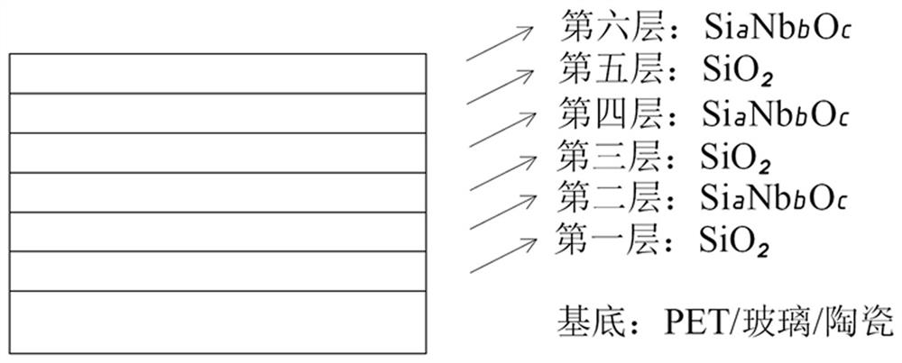
[0021] A hybrid mixed refractive index coating method of the present invention uses the ion-cleaned PET sheet as the substrate, and the film system is composed of SiO 2 、Si a Nb b o c (or Si p Ti q o r ) and so on, where Si a Nb b o c or (Si p Ti q o r ) and other dielectric materials can be adjusted and changed through equipment parameters. For example, in the magnetron sputtering equipment, a 2.0kw (1-18kw range is acceptable) power is applied above the Si target, and a 12.0Kw (1-18kw range is acceptable) power is applied above the Nb target, which can form a small amount of Si impurities. Si a Nb b o c Hybrid hybrid coating, which has a refractive index of about 2.22, which is lower than that of Nb 2 o 5 2.34. The film layer structure from the first layer to the sixth layer is: SiO 2 、Si a Nb b o c , SiO 2 、Si a Nb b o c , SiO 2 、Si a Nb b o c . Among them, 1≤a≤3, 0≤b≤3, 1≤c≤10, 1≤p≤3, 0≤q≤3, 1≤r≤10. Its film layer is a golden coating system, ...
Embodiment 2
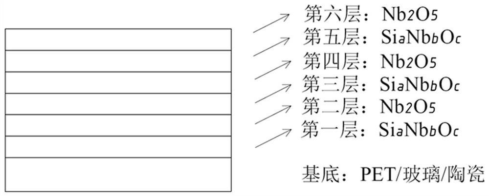
[0038] The invention relates to a hybrid mixed refractive index coating method, which mainly explains the function of the coating method in adjusting the stress of the film layer. Such as figure 2 As shown, PET or glass material is used as the substrate, and the constituent material is SiO 2 / Si a Nb b o c The high-brightness turquoise film system is used as the low refractive index layer, Nb 2 o 5 Do high refractive index layer, SiO 2 Pure material than Nb 2 o 5 The internal stress is much larger, and the SiO film with equal thickness is generally sputtered. 2 Thin layer stress value is about Nb 2 o 5 more than six times that of Si doped with Nb molecules a Nb b o c Material can effectively reduce stress. In this example, using Si a Nb b o c / Nb 2 o 5 Do low / high refractive index layer, compared to traditional SiO 2 / Nb 2 o 5 Structure, can effectively reduce internal stress, very suitable for surface coating of flexible substrates. The film layer stru...
PUM
| Property | Measurement | Unit |
|---|---|---|
| Peel force | aaaaa | aaaaa |
Abstract
Description
Claims
Application Information