
Preparation method of antireflection film allowing wide-angle incidence of infrared optical waveband in silicon or germanium base

A technology in infrared optics and substrates, used in sputtering, ion implantation, metal material coating, etc. The problems of reduced capacity, difficult film system design and process, etc., can achieve the effect of high film layer firmness and high density, temperature shock resistance, deliquescence resistance and laser damage resistance, and high density.

Inactive Publication Date: 2015-04-29
SOUTH WEST INST OF TECHN PHYSICS
View PDF3 Cites 5 Cited by
  • Summary
  • Abstract
  • Description
  • Claims
  • Application Information

AI Technical Summary

Problems solved by technology

However, in the prior art, there are few types of infrared film materials that can be used for wide-band high-reflection films involving infrared, and the design and process of film systems are very difficult.
And the existing infrared optical coating technology can only choose such as: ZnS, ZnSe, YbF 3 , ThF 4 , MgF 2 , LiF, CaF 2 , Si, Ge and other materials are used as coating materials to ensure that the film layer is firm
When the conventional coating is used and placed in a humid environment, the surface is in contact with air moisture, the transmittance and water resistance of the high anti-reflection coating will gradually decrease, and the anti-laser damage ability of the coating will gradually decrease, so it cannot be used in harsh outdoor environments for a long time. use

Method used


Image

  • Preparation method of antireflection film allowing wide-angle incidence of infrared optical waveband in silicon or germanium base
  • Preparation method of antireflection film allowing wide-angle incidence of infrared optical waveband in silicon or germanium base
  • Preparation method of antireflection film allowing wide-angle incidence of infrared optical waveband in silicon or germanium base

Examples


Embodiment 1

[0022] According to the present invention, first use the advanced optical thin film design software (TFCalc) of the United States to design the optimized film system that meets the technical index requirements of the present invention. Coating on the surface of the optically processed silicon material, use the film system design formula: G / 0.2L(5H5L)^50.2L / Air to optimize and calculate the optical thickness value of each layer of film and list them in order. In the formula, G is the substrate of silicon material, L is the refractive index N L Al = 1.60 2 o 3 Film material, H is the refractive index N H = ZnS film material of 2.20, Air is the refractive index N A = 1 air medium, film system reference wavelength λ c = 800nm. The above H and L are granular film materials with a purity of 99.9%. Specific steps include:

[0023] (1) For a hard moisture-proof film layer based on silicon or germanium materials and insulating the surface of silicon or germanium materials from c...

Embodiment 2

[0051] According to the optical thickness value of each layer of 9 layers of film design in the following table 2, repeat the method of experimental embodiment 1, adopt the optimal film system formula of the present invention and each layer optical thickness of table 2, in the coating process step:

[0052] (1) repeat process step (1) in embodiment 1;

[0053] (2) repeat process step (2) in embodiment 1;

[0054] (3) repeat process step (3) in embodiment 1;

[0055] (4) repeat process step (4) in embodiment 1;

[0056] (5) repeat process step (5) in embodiment 1;

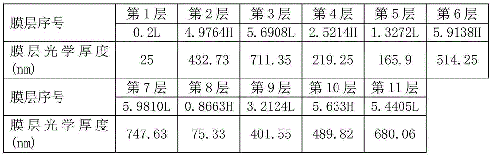
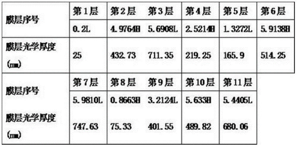
[0057] The actual optical thickness of each layer recorded after the coating is completed is shown in Table 2:

[0058] Table 2 (the optical thickness value table of the germanium 9-layer film that embodiment 2 is actually plated)

[0059]

[0060] Note: The value after the decimal point is not taken, because the precision is enough to meet the design plan.

[0061] (6) Annealing treatment: repeat process st...


PUM


Abstract

The invention discloses a preparation method of an antireflection film allowing the wide-angle incidence of infrared optical wavebands in a silicon or germanium base. Through the utilization of the preparation method disclosed by the invention, the design and the plated preparation of the antireflection film allowing the wide-range high-quality wide-angle range incidence of intermediate infrared optical wavebands of 3 micrometers to 5 micrometers can be realized, so that the firmness capability of a film layer is improved, and the service life of the film layer in the bad wild environment is prolonged. The technical scheme of the preparation method disclosed by the invention is realized by the following steps: (1) using a silicon or germanium material as a base, and calculating the optical thickness value of each film by a film system formula: G / 0.2L(5H5L) -50.2L / Air; attacking the base by an ion source before film plating and during film plating; (5) placing ZnS and Al2O3 film materials in a rotary electronic-gun evaporation source crucible, and finishing film plating by an optical vacuum film plating machine according to the thickness value calculated by the film system formula. The preparation method disclosed by the invention solves the difficult technological problem that when nonmetal or non-semiconductor film materials are used on the silicon or germanium base, the plated film is not firm and is difficult to reach high transmittance. The antireflection film prepared by the preparation method disclosed by the invention has the characteristics that the film layer firmness is high, and the transmittance of the wide-angle range incidence can reach 99%.

Description

technical field [0001] The invention relates to a method for coating an optical thin film, more specifically, the invention relates to a method for coating a silicon or germanium substrate with a mid-infrared 3um-5um optical band wide angle range incident anti-reflection coating. Background technique [0002] As a kind of optical film, anti-reflection coating is widely used in various optical and infrared components, solar cells and high-power laser systems. Anti-reflection coating can not only be used in pure optical devices, but also in modern science and technology, especially information The development of optical imaging technology and laser technology can also be widely used in optoelectronic and optical communication devices. At present, there are many different types of anti-reflection coatings that can meet some practical applications in the field of optical and infrared technology. However, the requirements for the comprehensive performance of anti-reflection coat...

Claims


Application Information

Patent Timeline
IPC IPC(8): C23C14/30C23C14/58C23C14/08C23C14/06
CPCC23C14/30C23C14/06C23C14/08C23C14/584
Inventor 王平秋张玉东杨柳于清代礼密林莉吉林陈蔚
Owner SOUTH WEST INST OF TECHN PHYSICS
Features
  • Generate Ideas
  • Intellectual Property
  • Life Sciences
  • Materials
  • Tech Scout
  • Unparalleled Data Quality
  • Higher Quality Content
  • 60% Fewer Hallucinations
Learn More