Insulated gate bipolar transistor

A technology of bipolar transistors and insulated gates, applied in semiconductor devices, electrical components, circuits, etc., can solve problems such as weakening device direction recovery performance, difficulty in manufacturing process control, and reducing on-resistance, so as to suppress minority carrier injection and reduce high-frequency power. power consumption and reduce on-resistance

Inactive Publication Date: 2022-03-29
朱江
View PDF0 Cites 1 Cited by
  • Summary
  • Abstract
  • Description
  • Claims
  • Application Information

AI Technical Summary

Problems solved by technology

[0003] Ideal insulated gate bipolar transistors require low turn-on voltage to reduce on-resistance, and at the same time require relatively fast and gentle reverse recovery performance; among them, in order to reduce the turn-on voltage drop of the device, it is necessary to transfer the P-type emitter region to the N-type base region A large number of minority carriers are injected to generate conductance modulation and reduce the resistance of the device in the on-state, but this causes the device to weaken the direction recovery performance; it is proposed to thin the back and implant a thin lightly doped P-type emitter region on the back of the N-type base region. , so as to reduce minority carrier injection, but at the same time, the chip is too thin, which brings difficulties to the manufacturing process control

Method used


Image

  • Insulated gate bipolar transistor
  • Insulated gate bipolar transistor
  • Insulated gate bipolar transistor

Examples


Embodiment 1

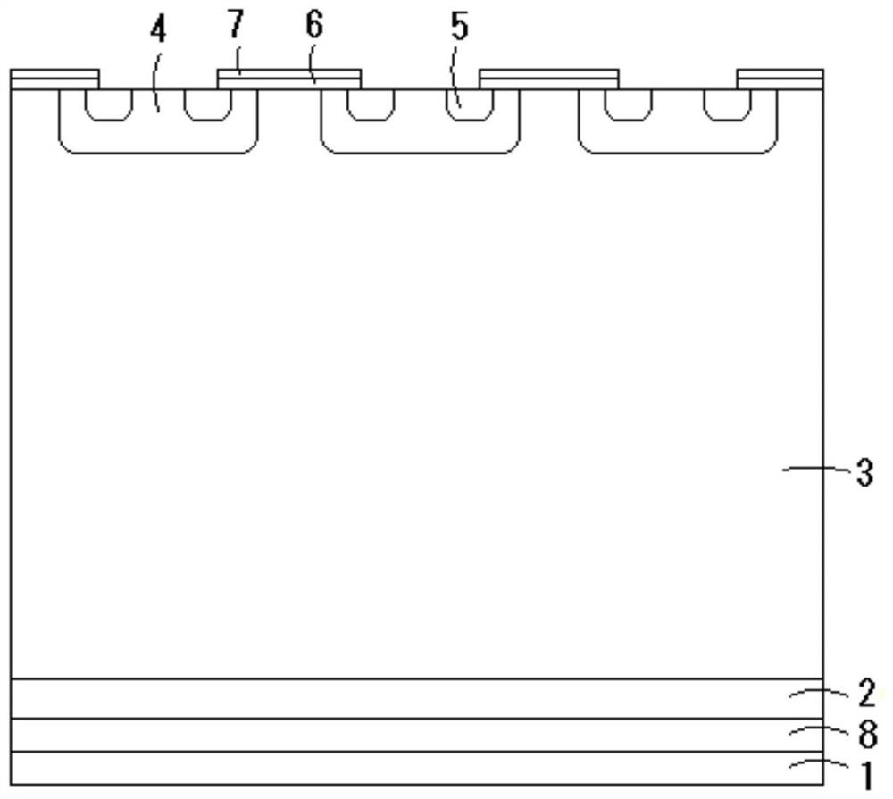
[0032] figure 1 It is a schematic cross-sectional view of the first type of upper surface planar structure insulated gate bipolar transistor of the present invention, combined below figure 1 The semiconductor device of the present invention will be described in detail.

[0033] An insulated gate bipolar transistor, the rear P+ emitter region 1 is made of P conductivity type polysilicon material, the thickness is 0.3-300um, and the doping concentration of boron atoms is 5E17cm -3; The N-type adjustment region 8 is made of N-conduction type polysilicon material with a thickness of 0.3-300um and a doping concentration of phosphorus atoms of 1E17cm -3 , located on the back P+ emitter region; N+ buffer layer 2, located on the N-type adjustment region, is a semiconductor silicon material of N conductivity type, and the doping concentration of phosphorus atoms is 5E13cm -3 ~1E16cm -3 , with a thickness of 10um; N-base region 3, located on the N+ buffer layer 2, is a semiconductor ...

Embodiment 2

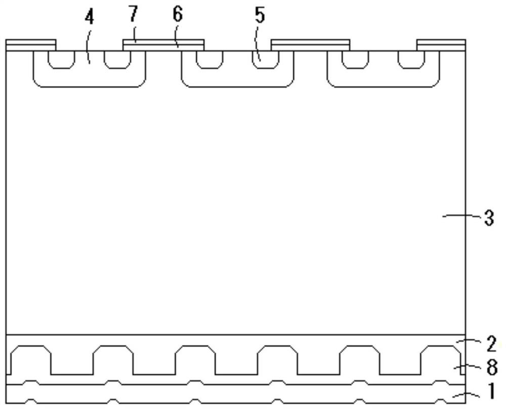
[0038] image 3 It is a cross-sectional view of the second back trench structure insulated gate bipolar transistor of the present invention, combined below image 3 The semiconductor device of the present invention will be described in detail.

[0039] An insulated gate bipolar transistor, the rear P+ emitter region 1 is made of P conductivity type polysilicon material, and the doping concentration of boron atoms is 5E17cm -3 , located on the lower surface of the N-type adjustment region 8; the N-type adjustment region 8 is made of N-conduction type polysilicon material, and the doping concentration of phosphorus atoms is 1E17cm -3 , located in the back trench in the N+ buffer layer 2; the N+ buffer layer 2, located above the N-type adjustment region, is a semiconductor silicon material of N conductivity type, and the doping concentration of phosphorus atoms is 5E13cm -3 ~1E16cm -3 , with a thickness of 30um, multiple trenches are set on the back of the N+ buffer layer; the...


PUM


Abstract

The invention provides an insulated gate bipolar transistor, which is characterized in that an N-type adjusting region is arranged between a substrate P + emitter region and an N-type base region, N-type conductive impurities are doped with polycrystalline or amorphous semiconductor materials, the N-type adjusting region inhibits minority carrier injection, and the number of minority carriers in the N-type base region is controlled and reduced; according to the invention, a device can be manufactured on a thick substrate slice, and minority carrier injection of a P-type emitter region at the back of the insulated gate bipolar transistor is inhibited; high-frequency characteristics of the device are improved and power consumption of the device is reduced.

Description

technical field [0001] The invention relates to insulated gate bipolar transistors in power semiconductors. Background technique [0002] Insulated Gate Bipolar Transistor (IGBT) is a combination of gate voltage control characteristics of metal oxide semiconductor field effect transistor (MOSFET) and low on-resistance characteristics of bipolar transistor (BJT). Semiconductor power devices have the characteristics of voltage control, large input impedance, low driving power, small on-resistance, low switching loss and high operating frequency. They are ideal semiconductor power switching devices and have broad development and application prospects. Generally speaking, from the front structure of the IGBT, the IGBT can be divided into two types: planar type and trench gate type; from the breakdown characteristics of the IGBT, it can be divided into two types: the punch-through type and the non-punch-through type. The P+ surface on the back of the device has an N+ buffer laye...

Claims


Application Information

Patent Timeline
Patent Type & Authority Applications(China)
IPC IPC(8): H01L29/739H01L29/06
CPCH01L29/7393H01L29/0603H01L29/0684
Inventor 不公告发明人
Owner 朱江
Why Eureka
Try Eureka