Thickness measuring structure and measuring method for aluminum-gallium-nitrogen barrier layer
A technology of thickness measurement and barrier layer, applied in semiconductor/solid-state device testing/measurement, electrical components, electric solid-state devices, etc., can solve problems such as poor Schottky contact, unknown proportion of Al composition, large error, etc. Achieve high accuracy and consistency, simple and easy-to-operate measurement method
- Summary
- Abstract
- Description
- Claims
- Application Information
AI Technical Summary
Problems solved by technology
Method used
Image
Examples
Embodiment 1
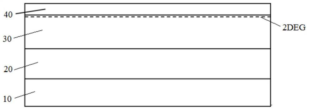
[0062] ginseng figure 1 As shown, the AlGaN barrier layer thickness measurement structure in this embodiment includes
[0063] Substrate 10, substrate is silicon (Si), sapphire (Al 2 o 3 ), silicon carbide (SiC), etc.;
[0064] The heterojunction located on the substrate, the heterojunction includes a gallium nitride channel layer 30 and an aluminum gallium nitride barrier layer 40, and two Dimensional electron gas (Two-dimensional electron gas, 2DEG), the thickness of the gallium nitride channel layer is 50nm ~ 2μm, the aluminum gallium nitrogen barrier layer is Al x Ga 1-x The N (x=0.1-0.3) barrier layer has a thickness of 10nm-50nm.
[0065] The measurement structure in this embodiment also includes a buffer layer 20 located between the substrate and the heterojunction. The buffer layer is mainly made of nitride, including gallium nitride, aluminum nitride, aluminum gallium nitride and the like.
[0066] Further, an isolation layer, such as an AlN spacer, is formed be...
Embodiment 2
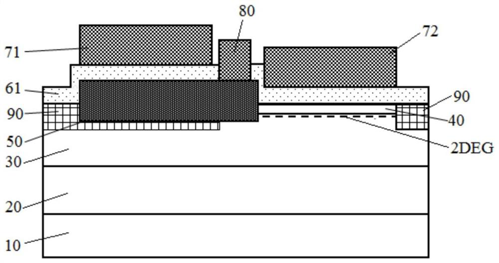
[0098] In an actual process, the thickness of the first passivation layer may be small, and the test structure group can be increased by using the second passivation layer, and the test results of multiple groups of test structures can be compared and verified.
[0099] combine Figure 4 As shown, the measurement structure in this embodiment is substantially the same as that in Embodiment 1, except that a second passivation layer 62 is formed on the first passivation layer 61 .
[0100] The material of the second passivation layer can be an insulating medium such as silicon nitride, silicon oxide or polyimide, or a composite medium composed of various insulating mediums, and the thickness can be 100 nm˜1 μm.
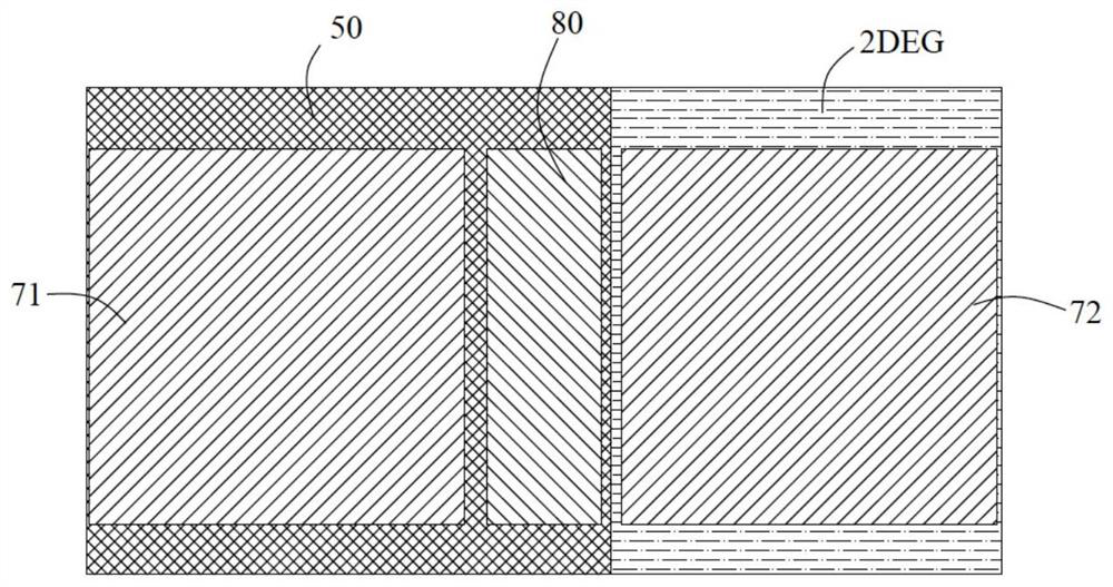
[0101] ginseng Figure 5 Shown is a top view of the measurement structure. The left area is the upper plate of the first parallel plate capacitor, and the right area is the upper plate of the second parallel plate capacitor. The lower plates of the two capacitors pass t...
PUM
| Property | Measurement | Unit |
|---|---|---|
| thickness | aaaaa | aaaaa |
| thickness | aaaaa | aaaaa |
| thickness | aaaaa | aaaaa |
Abstract
Description
Claims
Application Information


