Laser processing and real-time in-situ high-resolution observation device of micro-nano structure

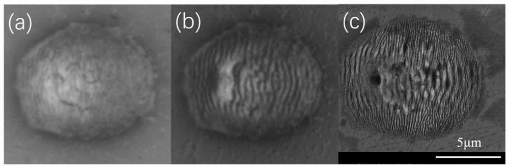
A laser processing, micro-nano structure technology, applied in measurement devices, optics, microscopes, etc., can solve problems affecting LIPSS formation, image distortion, increase chromatic aberration and spherical aberration of the imaging system, and expand the valuable observation area, intuitive and reliable. Observation means, the effect of avoiding spherical aberration and chromatic aberration

Pending Publication Date: 2022-04-12
JIANGSU UNIV
View PDF1 Cites 2 Cited by
  • Summary
  • Abstract
  • Description
  • Claims
  • Application Information

AI Technical Summary

Problems solved by technology

The problem with method (1) is that different laser parameters need to be irradiated at different positions on the sample surface during processing, and by comparing the LIPSS structure at different positions, the formation mechanism of LIPSS can be speculated
However, before being irradiated with laser light, the microscopic topography of the sample surface cannot be completely the same. Some small defects and structural differences on the sample surface will affect the formation of LIPSS, which is of great importance for the study of the influence of laser parameters on LIPSS. Then analyze the formation mechanism of LIPSS to cause interference
The problem with method (2) is: in order to improve the spatial resolution of microscopic imaging, large numerical aperture and high-power microscopic objective lenses are usually used for processing and observation, but the focal spot of the processed light is only about 1 micron after being focused by the high-power microscopic objective lens , there are only 1-3 LIPSS in the focal spot area
However, the introduction of the concave lens in the imaging optical path increases the chromatic aberration and spherical aberration of the imaging system, causing image distortion and reducing the imaging quality

Method used


Image

  • Laser processing and real-time in-situ high-resolution observation device of micro-nano structure
  • Laser processing and real-time in-situ high-resolution observation device of micro-nano structure

Examples


Embodiment Construction

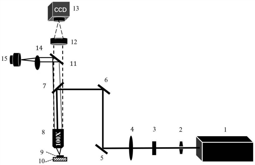
[0026] The present invention will be further described below in conjunction with the accompanying drawings and specific embodiments, but the protection scope of the present invention is not limited thereto.

[0027] Embodiments of the present invention are described in detail below, examples of which are shown in the drawings, wherein the same or similar reference numerals designate the same or similar elements or elements having the same or similar functions throughout. The embodiments described below by referring to the figures are exemplary and are intended to explain the present invention and should not be construed as limiting the present invention.

[0028] In describing the present invention, it is to be understood that the terms "central", "longitudinal", "transverse", "length", "width", "thickness", "upper", "lower", "axial", The orientation or positional relationship indicated by "radial", "vertical", "horizontal", "inner", "outer", etc. is based on the orientation o...


PUM

PropertyMeasurementUnit
lengthaaaaaaaaaa
wavelengthaaaaaaaaaa

Abstract

The invention provides a laser processing and real-time in-situ high-resolution observation device of a micro-nano structure, which comprises a laser, a CCD (Charge Coupled Device) camera and a light source, the laser is focused on a sample through a laser processing light path, and the light source obliquely irradiates the sample through an illumination light path and is reflected into the CCD camera through a microscopic imaging light path; a laser beam sequentially passes through an electronic shutter, a gradual-change neutral optical filter, a long-focus lens, a reflecting mirror group, a dichroscope and a microobjective and is focused on a sample, so that a laser processing light path is formed; illumination light sequentially passes through the short-focus lens, the beam splitter, the dichroscope and the microscope objective and obliquely irradiates a sample to form an illumination light path; illuminating light reflected by the sample sequentially passes through the microscope objective, the dichroscope and the beam splitter and enters the CCD camera, and a microscopic imaging light path is formed. Short-wavelength illumination light is adopted on an illumination light path, the imaging quality is improved in a mode of illuminating a sample in an oblique incidence mode, and in-situ observation on the surface of a material in the machining process is achieved.

Description

technical field [0001] The invention relates to the fields of laser microprocessing and microscopic imaging, in particular to a laser processing and real-time in-situ high-resolution observation device for micro-nano structures. Background technique [0002] The interaction between laser and metals, semiconductors, dielectrics and other materials will induce various micro-nano structures on the surface of materials, including micro-nano cone arrays, micro-nano island arrays, and periodic surface micro-nano structures (Laser-Induced Periodic Surface Structures, LIPSS) etc. These micro-nanostructures play an important role in material modification. In particular, the structure of LIPSS has been widely studied since it was first reported in 1965, and has been found to have composite functions such as anti-reflection, coloring, enhanced Raman scattering, hydrophobic and oleophobic, anti-corrosion, anti-wear and drag reduction, and antibacterial. It has great application potenti...

Claims


Application Information

Patent Timeline
Patent Type & Authority Applications(China)
IPC IPC(8): G01N23/2251G02B21/06G02B21/36
Inventor 宋娟王宏剑
Owner JIANGSU UNIV
Why Eureka
Try Eureka