
Clock-driven FPGA chip global layout method based on multi-electric-field model

A global layout, clock-driven technology, applied in electrical digital data processing, instrumentation, computing and other directions, can solve the problems affecting the quality of layout results, can not achieve good layout quality, poor results, etc., to achieve good computing efficiency and layout results quality effect

Active Publication Date: 2022-04-12
PEKING UNIV
View PDF4 Cites 0 Cited by
  • Summary
  • Abstract
  • Description
  • Claims
  • Application Information

AI Technical Summary

Problems solved by technology

[0006] (1) Existing FPGA layout tools do not work well on large-scale FPGA layout problems
The existing FPGA layout tools mainly use the global layout algorithm based on quadratic programming. However, with the continuous increase of chip size and chip complexity, the FPGA global layout algorithm based on quadratic programming cannot achieve very good results in large-scale FPGA layout problems. good layout quality
[0007] (2) Existing FPGA global layout algorithms seldom consider restrictions on clock signal routing in the global layout stage
Due to the lack of restrictions on clock signal routing in the layout stage, the position of some devices that violate the clock signal routing needs to be adjusted in the later legalization stage, which will affect the quality of the entire layout result
[0008] In summary, the existing traditional FPGA global layout algorithm is difficult to achieve good layout results on large-scale FPGA layout problems, and because the restrictions on clock signal routing are less considered in the global layout stage, the legalization in the later stage of layout Adjustment of devices in stages that violate clock routing signals can affect placement quality

Method used


Image

  • Clock-driven FPGA chip global layout method based on multi-electric-field model
  • Clock-driven FPGA chip global layout method based on multi-electric-field model
  • Clock-driven FPGA chip global layout method based on multi-electric-field model

Examples


Embodiment Construction

[0028] Below in conjunction with the accompanying drawings, the present invention is further described by means of embodiments, but the scope of the present invention is not limited in any way.

[0029] The high-efficiency clock-driven FPGA global layout algorithm based on the multi-electric field system provided by the invention has the input including the circuit netlist and the FPGA chip layout constraints, and outputs the FPGA global layout result considering the clock routing constraints.

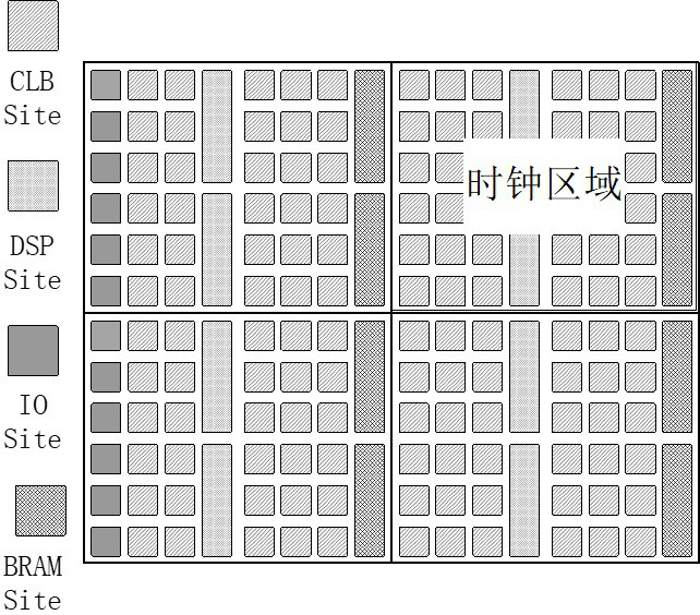
[0030] The following first provides a description of the input of the present invention. In the present invention, the circuit netlist uses said, of which represents a collection of devices, Represents a collection of hyperedges between devices. Note that in the FPGA layout problem, a hyperedge Multiple devices can be connected simultaneously. Each device has its own type. In this embodiment, the possible types of the device are a look-up table (Look-up Table, hereinafter refe...


PUM


Abstract

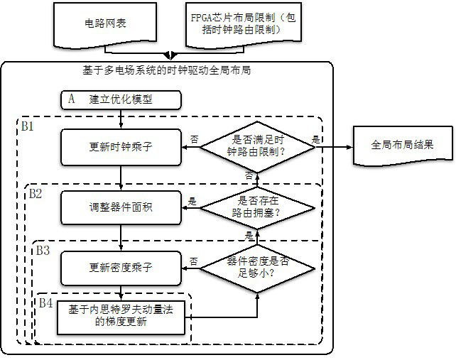
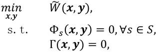
The invention discloses a clock-driven FPGA chip global layout method based on a multi-electric field model. The method comprises the following steps: respectively establishing electric field models for density distribution of various different device types; inputting a circuit netlist obtained after logic synthesis and layout limitation of the FPGA chip, so that a layout result which is beneficial to meeting clock routing limitation in a legalization stage is generated in a global layout stage; converting the constrained non-convex optimization model into an unconstrained non-convex optimization model; and solving the constraint uniformly by adopting a nested optimization framework method, namely realizing the clock-driven FPGA chip global layout based on the multi-electric-field model. In addition, the method also adopts an algorithm structure suitable for the GPU to perform parallel computation, and the GPU can be fully utilized to perform accelerated computation, so that a better layout result meeting clock routing limitation is efficiently obtained in a global layout stage, and the quality and effect of the global layout of the FPGA chip are improved.

Description

technical field [0001] The invention belongs to the technical field of Electronic Design Automation (hereinafter referred to as EDA), relates to a global layout technology for Field Programmable Gate Array (hereinafter referred to as FPGA) in the physical design of chip integrated circuits, and specifically relates to a A clock-driven FPGA global layout method based on a multi-electric field model system. Background technique [0002] An FPGA is a semi-custom integrated circuit chip with programmable features that is pre-designed on a silicon chip. In the FPGA chip manufacturing process, the manufacturer will design the programmable gate logic device on the silicon chip in advance; when the customer uses the process, the designer can describe the customized logic circuit through hardware description language (Verilog or VHDL), and then use the hardware description language (Verilog or VHDL) to describe the customized logic circuit. EDA software such as logic synthesis, plac...

Claims


Application Information

Patent Timeline
IPC IPC(8): G06F30/347G06F30/343
CPCY02E60/00
Inventor 林亦波麦景
Owner PEKING UNIV
Learn More