Semiconductor structure and forming method thereof

A semiconductor and conductive column technology, applied in the field of semiconductor structure and its formation, can solve the problem that the capacitance value of the capacitor needs to be improved urgently, and achieve the effect of increasing the capacitance value and increasing the surface area

Pending Publication Date: 2022-04-12
CHANGXIN MEMORY TECH INC
View PDF0 Cites 0 Cited by
  • Summary
  • Abstract
  • Description
  • Claims
  • Application Information

AI Technical Summary

Problems solved by technology

The capacitance value of the capacitor needs to be improved urgently

Method used


Image

  • Semiconductor structure and forming method thereof
  • Semiconductor structure and forming method thereof
  • Semiconductor structure and forming method thereof

Examples


Embodiment Construction

[0050] As mentioned in the background, the capacitance value of the existing semiconductor structure still needs to be improved.

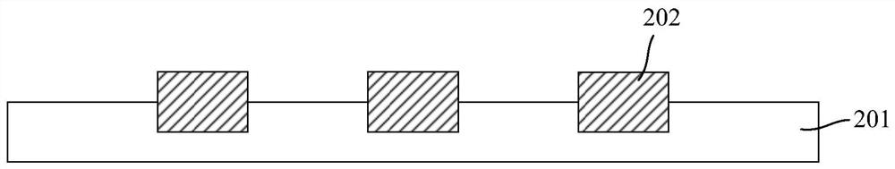
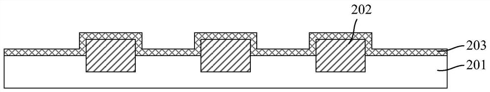
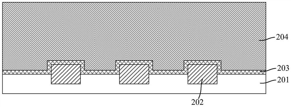
[0051] To this end, the present invention provides a semiconductor structure and a method for forming the same. The method includes: providing a substrate; forming a plurality of lower electrodes on the substrate, and the lower electrodes include ring-shaped wall and petal-shaped wall, and the petal-shaped wall divides the interior of the annular wall into several discrete first openings; a dielectric layer is formed on the bottom and side walls of the first opening; An upper electrode is formed in the opening, and the dielectric layer is located between the lower electrode and the upper electrode. The lower electrode of the present invention includes a ring-shaped wall and a petal-shaped wall, so that the surface area of ​​the lower electrode increases, and when the dielectric layer and the corresponding upper electrode are subsequently formed on ...


PUM


Abstract

The invention discloses a semiconductor structure and a forming method thereof, and the method comprises the steps: forming a plurality of lower electrodes on a substrate, each lower electrode comprises an annular wall and a petal-shaped wall which extend in a direction perpendicular to the surface of the substrate, and the petal-shaped walls divide the interior of the annular wall into a plurality of discrete first openings; forming a dielectric layer on the bottom and the side wall of the first opening; and forming an upper electrode in the first opening, wherein the dielectric layer is located between the lower electrode and the upper electrode. The lower electrode comprises the annular wall and the petal-shaped wall, so that the surface area of the lower electrode is increased, when the dielectric layer and the corresponding upper electrode are subsequently formed on the lower electrode, the surface area of the dielectric layer and the surface area of the upper electrode are correspondingly increased, and therefore the capacitance value of the formed semiconductor structure is increased.

Description

technical field [0001] The invention relates to the field of semiconductor manufacturing, in particular to a semiconductor structure and a forming method thereof. Background technique [0002] Dynamic Random Access Memory (Dynamic Random Access Memory, DRAM) is a semiconductor storage device commonly used in computers, and is composed of many repeated storage units. Each memory cell usually includes a capacitor and a transistor. The gate of the transistor is connected to the word line, the drain is connected to the bit line, and the source is connected to the capacitor. The voltage signal on the word line can control the opening or closing of the transistor, and then through the bit line Read the data information stored in the capacitor, or write the data information into the capacitor through the bit line for storage. [0003] As the manufacturing process continues to evolve, the integration level of DRAM continues to increase, the size of components continues to shrink, a...

Claims


Application Information

Patent Timeline
Patent Type & Authority Applications(China)
IPC IPC(8): H01L21/8242H01L27/108
CPCH01L28/90H10B12/033
Inventor 胡建城
Owner CHANGXIN MEMORY TECH INC
Why Eureka
Try Eureka