
Transconductance unit circuit

A transconductance unit and circuit technology, applied in the direction of amplifier input/output impedance improvement, DC-coupled DC amplifier, differential amplifier, etc., can solve the problems of advanced technology not suitable for power supply voltage, complex circuit composition structure, inconsistent mass production, etc. Achieve good linearity, more linearity, and increase the output range

Pending Publication Date: 2022-04-12
SHANGHAI PANCHIP MICROELECTRONICS CO LTD
View PDF0 Cites 0 Cited by
  • Summary
  • Abstract
  • Description
  • Claims
  • Application Information

AI Technical Summary

Problems solved by technology

[0003] like figure 1 As shown, it is a schematic circuit diagram of a transconductance unit that increases the output impedance by adding a Cascode (cascode) structure in the prior art. In order to achieve a large output impedance, a Cascode composed of transistors M3 and M4 is added to the transconductance unit. structure to increase the output impedance, but the Cascode structure achieves high output impedance by sacrificing the output range, resulting in a relatively small linear range, which is not suitable for advanced technology with lower power supply voltage VDD; in addition, the transconductance unit circuit passes the transistor M11 , M12 increases the input transconductance, and with the process changes, there will be great differences in the application of transistors M11 and M12 to different chips, so there will be inconsistencies in mass production, and the circuit composition structure is relatively complicated. Therefore, in view of the above problems, it is urgent It is necessary to design a transconductance unit circuit to meet the needs of actual use

Method used


Image

  • Transconductance unit circuit
  • Transconductance unit circuit
  • Transconductance unit circuit

Examples


Embodiment Construction

[0041] The following will clearly and completely describe the technical solutions in the embodiments of the present invention with reference to the accompanying drawings in the embodiments of the present invention. Obviously, the described embodiments are only some, not all, embodiments of the present invention. Based on the embodiments of the present invention, all other embodiments obtained by persons of ordinary skill in the art without creative efforts fall within the protection scope of the present invention.

[0042] It should be noted that, in the case of no conflict, the embodiments of the present invention and the features in the embodiments can be combined with each other.

[0043] The present invention will be further described below in conjunction with the accompanying drawings and specific embodiments, but not as a limitation of the present invention.

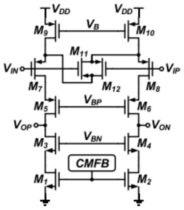
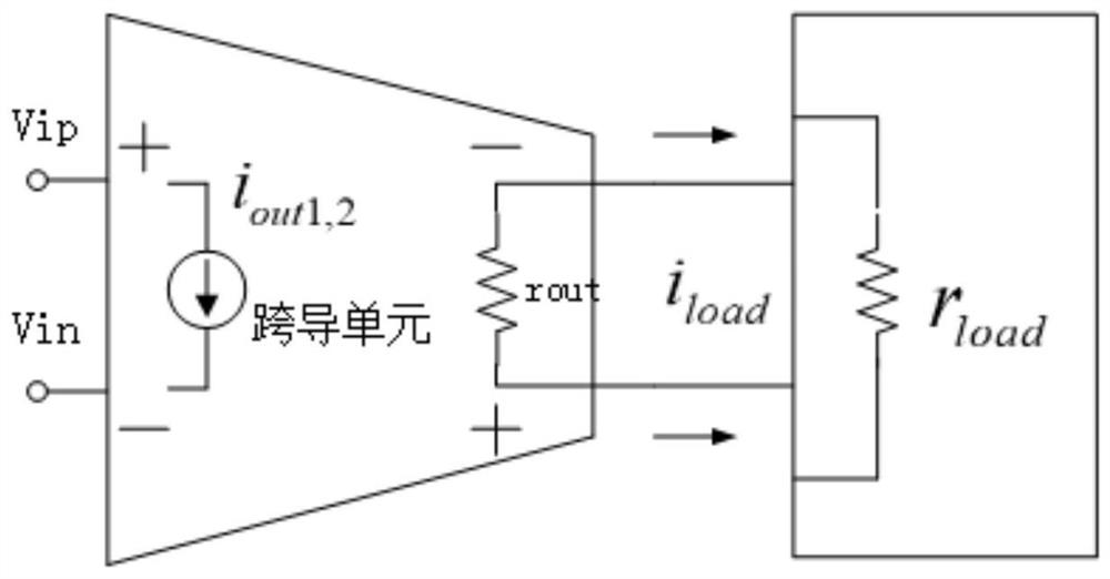
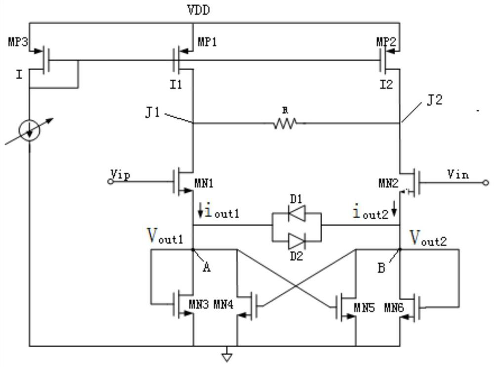
[0044] The invention provides a transconductance unit circuit, which belongs to the field of integrated circuit ...


PUM


Abstract

The invention discloses a transconductance unit circuit, which belongs to the field of integrated circuit design and comprises a first transistor connected between a first node and a first output end; the second transistor is connected between the second node and the second output end; the input compensation circuit is connected between the first node and the second node; the amplitude limiting circuit is used for limiting the output amplitude of the first output end or the second output end; the feedback circuit comprises a first feedback circuit which is controllably connected between a first output end and a grounding end under the action of a first feedback signal, and the first feedback signal is output by a second output end; and the second feedback circuit is controllably connected between the second output end and the grounding end under the action of a second feedback signal, and the second feedback signal is output by the first output end. According to the invention, the output impedance is increased through the feedback circuit; the output range and the linearity are increased through the amplitude limiting circuit; and the linearity of the input transconductance is better through the input compensation circuit.

Description

technical field [0001] The invention relates to the field of integrated circuit design, in particular to a transconductance unit circuit. Background technique [0002] Transconductance (GM) refers to the ratio of the output current of a circuit unit, usually an amplifier that converts voltage to current, to the input voltage to the unit. With the rapid progress of CMOS manufacturing technology, the feature size of the device is continuously reduced, and the power supply voltage is also continuously reduced, resulting in the limitation of the output impedance and linearity range of the transconductance unit realized by the classic differential pair. Usually we introduce source degeneration resistors in the differential pair structure to improve the linearity of the transconductance unit. On this basis, the transconductance of the input MOS pair tube is enhanced and the degradation depth is increased, which can further improve the linearity of the transconductance unit. [00...

Claims


Application Information

Patent Timeline
Patent Type & Authority Applications(China)
IPC IPC(8): H03F1/32H03F1/56H03F3/45
Inventor 黄继成徐冰妍
Owner SHANGHAI PANCHIP MICROELECTRONICS CO LTD
Learn More