

SiC substrate, SiC epitaxial substrate, SiC crystal ingot, and method for producing same
A manufacturing method and substrate technology, applied in chemical instruments and methods, semiconductor/solid-state device manufacturing, crystal growth, etc., can solve problems such as work performance and reliability impact
- Summary
- Abstract
- Description
- Claims
- Application Information
AI Technical Summary
Problems solved by technology
Method used
Image

Examples
Embodiment 1
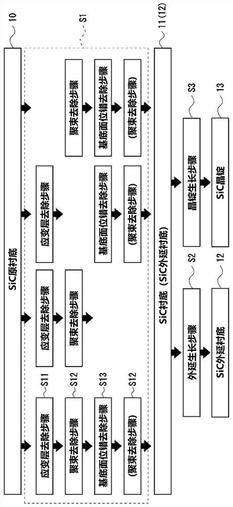
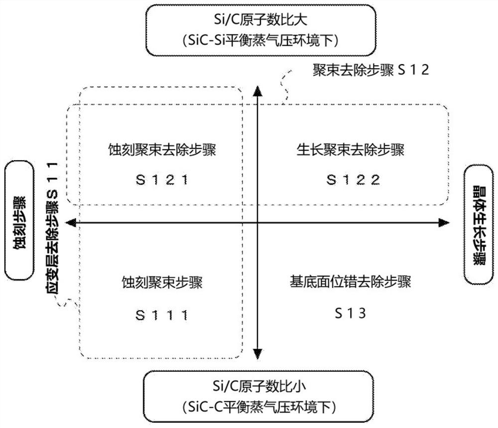
[0322] Embodiment 1 is an embodiment specifically illustrating the etching focusing step S111. Embodiment 2 is an embodiment specifically illustrating the etching beam removal step S121. Embodiment 3 is an embodiment specifically illustrating the growth beam removal step S122. Embodiment 4 is an embodiment specifically illustrating the basal plane dislocation reduction step S13.
Embodiment 5
[0323] Example 5 is an example specifically illustrating a crystal growth step for forming a voltage-resistant layer.
[0324]
[0325] The SiC original substrate 10 is accommodated in the main body container 20 and the high melting point container 40 (refer to Figure 9 ), and perform heat treatment under the following heat treatment conditions, thereby removing the strained layer 101 of the SiC original substrate 10 .
[0326] [SiC primary substrate 10]
[0327] Polymorph: 4H-SiC
[0328] Substrate size: width 10mm x width 10mm x thickness 0.45mm
[0329] Deviation direction and deviation angle: direction 4° deviation
[0330] Etched surface: (0001) crystal plane
[0331] Depth of strained layer 101: 5 μm
[0332] In addition, the depth of the strained layer 101 was confirmed by the SEM-EBSD method. In addition, this strained layer 101 can also be confirmed by TEM, μXRD, and Raman spectroscopy.
[0333] [Main container 20]
[0334] Material: Polycrystalline SiC
...
Embodiment 2
[0371]
[0372] The SiC original substrate 10 is accommodated in the main body container 20 and the high melting point container 40 (refer to Figure 11 ), and heat treatment was performed under the following heat treatment conditions, whereby the MSB on the surface of the SiC original substrate 10 was removed.
[0373] [SiC primary substrate 10]
[0374] Polymorph: 4H-SiC
[0375] Substrate size: width 10mm x width 10mm x thickness 0.3mm
[0376] Deviation direction and deviation angle: direction 4° deviation
[0377] Etched surface: (0001) crystal plane
[0378] With or without MSB: Yes
[0379] In addition, the step height, platform width, and the presence or absence of MSB can be confirmed by an atomic force microscope (AFM) or a scanning electron microscope (SEM) image contrast evaluation method described in JP-A-2015-179082.
[0380] [Main container 20]
[0381] Material: Polycrystalline SiC
[0382] Container size: diameter 60mm x height 4mm
[0383] Material...
PUM
| Property | Measurement | Unit |
|---|---|---|
| thickness | aaaaa | aaaaa |
| depth | aaaaa | aaaaa |
Abstract
Description
Claims
Application Information