
Packaging, aligning and laminating device and packaging, aligning and laminating control method

A bonding device and accommodating technology, which is applied in the direction of instruments, nonlinear optics, optics, etc., can solve the problems of narrow frame glue for sealing liquid crystals, difficulty in uniform thickness of liquid crystal cells, small size of LCoS devices, etc.

Active Publication Date: 2022-04-29
东莞市芯萌慧显电子科技有限公司
View PDF4 Cites 1 Cited by
  • Summary
  • Abstract
  • Description
  • Claims
  • Application Information

AI Technical Summary

Problems solved by technology

[0003] Compared with the preparation of traditional transmissive liquid crystal devices, the preparation of LCoS devices is more difficult. The difficulties in the preparation are mainly reflected in the smaller size of LCoS devices and the higher requirements for alignment and bonding accuracy of ITO glass and silicon substrates; the sealing of liquid crystals. The frame glue is narrower (about 500um), and spacers with a certain diameter are mixed in it, so it is more difficult to control the uniformity of the overall liquid crystal cell thickness in the process

Method used


Image

  • Packaging, aligning and laminating device and packaging, aligning and laminating control method
  • Packaging, aligning and laminating device and packaging, aligning and laminating control method
  • Packaging, aligning and laminating device and packaging, aligning and laminating control method

Examples


preparation example Construction

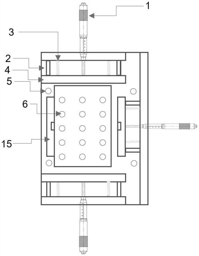
[0031] Compared with the preparation of traditional transmissive liquid crystal devices, the preparation of LCoS devices is more difficult. The difficulties are mainly reflected in the smaller size of LCoS devices, higher alignment precision requirements for ITO glass and silicon substrates; sealing liquid crystal frame glue Narrower (about 500um), which is mixed with spacers of a certain diameter, it is more difficult to control the uniformity of the overall cell gap in the process; the current mature LCoS process and equipment are basically monopolized by foreign countries, and there are basically no such production conditions in China , especially the LCoS process with a cell gap lower than 3um, is still being explored in China.

[0032] The packaging alignment bonding device and the packaging alignment bonding control method provided in the embodiments of the present application are mainly aimed at the verification stage of materials before mass production, packaging a sing...


PUM


Abstract

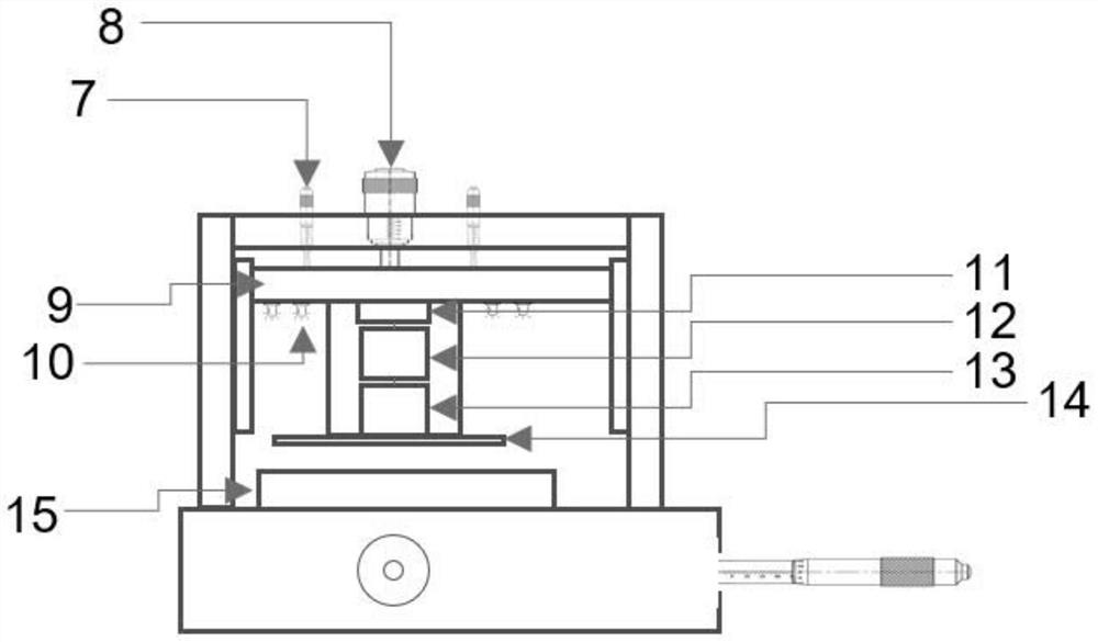
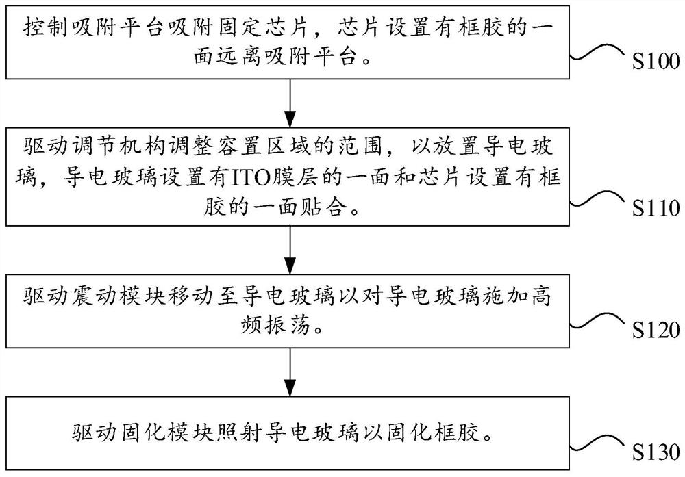
The invention provides a packaging, aligning and laminating device and a packaging, aligning and laminating control method, and relates to the technical field of semiconductor packaging, the packaging, aligning and laminating device comprises a support, the support comprises an adsorption platform used for fixing a chip, the periphery of the adsorption platform is provided with an adjusting mechanism and a baffle plate so as to form an accommodating area in an enclosing manner, conductive glass is arranged on the side, provided with the frame glue, of the chip through the containing area, and the adjusting mechanism adjusts the range of the containing area; a movable vibration module and a movable curing module are further arranged above the adsorption platform, the vibration module can move to the conductive glass and pressurize the conductive glass so as to transmit high-frequency oscillation to the frame glue between the chip and the conductive glass, spacers of the frame glue are distributed in a single-layer mode, and the uniformity of cell gap in the box pressing process is improved; the curing module is used for providing radiation energy for the frame glue to cure the frame glue. And a box pressing process and a curing process are integrated together, so that the yield, the efficiency and the reliability of an LCOS packaging test are realized.

Description

technical field [0001] The present application relates to the technical field of semiconductor packaging, and in particular to a packaging alignment bonding device and a control method for packaging alignment bonding. Background technique [0002] Liquid Crystal on Silicon (LCoS) is a reflective microdisplay device. Compared with transmissive liquid crystal, it has the advantages of small size, high resolution and high light utilization rate (high aperture ratio), especially the pure phase modulation type. LCoS spatial light modulator, because it can flexibly and conveniently modulate the light wave front, has extremely important applications in the fields of optical communication, digital holography, micro-optics, etc. It is a wavelength selective switch (WSS), maskless lithography system, holography The core component of the optical tweezers system. [0003] Compared with the preparation of traditional transmissive liquid crystal devices, the preparation of LCoS devices i...

Claims


Application Information

Patent Timeline
Patent Type & Authority Applications(China)
IPC IPC(8): G02F1/1339
CPCG02F1/1339
Inventor 何军胡健
Owner 东莞市芯萌慧显电子科技有限公司
Learn More