Method for connecting graphite film and copper

A connection method and technology of graphite film, applied in welding equipment, manufacturing tools, non-electric welding equipment, etc., can solve problems such as easy cracks, high melting point of graphite film, and inability to form intermetallic compounds, so as to reduce residual stress and reduce welding The effect of seam width

Active Publication Date: 2022-05-03
HARBIN INST OF TECH AT WEIHAI
View PDF14 Cites 1 Cited by
  • Summary
  • Abstract
  • Description
  • Claims
  • Application Information

AI Technical Summary

Problems solved by technology

However, there are many difficulties in the welding of graphite film and copper: (1) The graphite film has a high melting point, and fusion welding cannot be used; (2) The thermal expansion coefficient difference between graphite film and copper is too large, and cracks are easy to occur; (3) The wettability of graphite film is not ...

Method used


Image

  • Method for connecting graphite film and copper
  • Method for connecting graphite film and copper

Examples


Embodiment 1

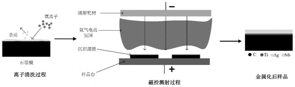
[0025] A method for diffusion connection between a high thermal conductivity graphite film and copper in this embodiment includes the following steps:

[0026] Step 1. Put the high thermal conductivity graphite film into the acetone solution and ultrasonically clean it for 10min-20min to remove the oil stains and impurities on the surface;

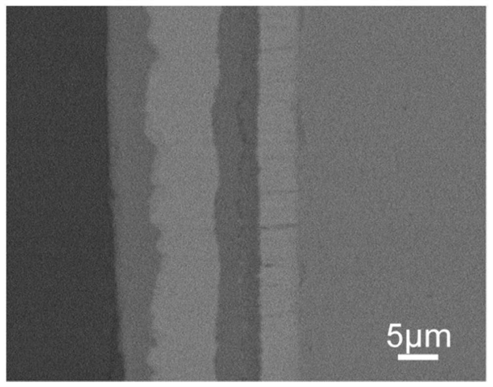
[0027] Step 2: Place the graphite film obtained in step 1 in a magnetron sputtering chamber, control the temperature to room temperature, and evacuate to make the air pressure inside the chamber less than 5×10 -3 Pa, and then pass 3sccm of argon to maintain the pressure at 2 × 10 -3 Pa±0.5Pa, the bias voltage was adjusted to 400V, and the surface of the graphite film was bombarded with argon ions for 10min. This process was ion cleaning, and then magnetron sputtering was started; the parameters of the metal layer: the power was 350W, and the Ti-plating time was 60min. The Ag plating time is 20min, and the Nb plating time is 20min;

[002...

Embodiment 2

[0032] A method for diffusion connection between a high thermal conductivity graphite film and copper in this embodiment includes the following steps:

[0033] Step 1. Put the high thermal conductivity graphite film into the acetone solution and ultrasonically clean it for 10min-20min to remove the oil stains and impurities on the surface;

[0034] Step 2: Place the graphite film obtained in step 1 in a magnetron sputtering chamber, control the temperature to room temperature, and evacuate to make the air pressure inside the chamber less than 5×10 -3 Pa, and then pass 3sccm of argon to maintain the pressure at 2 × 10 -3 Pa±0.5Pa, the bias voltage is adjusted to 400V, and the surface of the graphite film is bombarded with argon ions for 10min. This process is ion cleaning, and then magnetron sputtering is started; the parameters of the metal layer: the power is 400W, and the Ti-plating time is 90min. The Ag plating time is 50min, and the Nb plating time is 60min;

[0035] Ste...


PUM


Abstract

The invention relates to the technical field of graphite film and metal connection, in particular to a solid-phase diffusion connection method capable of realizing connection of a graphite film and metal copper, effectively reducing the width of a welding seam and reducing the stress at a joint, which is characterized by comprising the following steps of: carrying out surface metallization treatment on the graphite film to form a metal intermediate layer on the surface of the graphite film; the metal copper and the metal intermediate layer are in diffusion connection to obtain a graphite film and metal complex, and the metallization treatment on the surface of the graphite film refers to forming a nano-scale or micron-scale metal intermediate layer on the surface of the graphite film by using a magnetron sputtering technology; according to the method, the magnetron sputtering technology and the diffusion bonding method are combined, solid-phase diffusion bonding is successfully applied to connection of the high-thermal-conductivity graphite film and copper, the width of a welding seam is effectively reduced, and due to the existence of a gradient interface layer in the welding seam, the residual stress of a connector caused by the large difference of thermal expansion coefficients of base metal on the two sides is effectively reduced.

Description

Technical field: [0001] The invention relates to the technical field of graphite film and metal connection, in particular to a solid phase diffusion connection method which can realize the connection between graphite film and metal copper, effectively reduce the width of the weld seam and reduce the stress at the joint. Background technique: [0002] In recent years, with the continuous development of AI technology and the arrival of the 5G data era, people's demand for intelligent electronic products has increased day by day and they have put forward higher and higher requirements for their intelligence. This promotes the rapid development of semiconductor and microelectronics technology, and miniaturization, light weight, high integration and high frequency have gradually become the development trend of microprocessor chips. With the high integration and miniaturization of microprocessor chips, the feature size of the chip is continuously reduced, the power per unit area i...

Claims


Application Information

Patent Timeline
IPC IPC(8): B23K20/00C23C14/35C23C14/18
CPCB23K20/00B23K20/001B23K20/002C23C14/35C23C14/185
Inventor 刘多陈斌赵可汗李星仪宋延宇宋晓国
Owner HARBIN INST OF TECH AT WEIHAI
Why Eureka
Try Eureka