

High-transmittance shadow-eliminating conductive glass and manufacturing method thereof
A technology of conductive glass and glass substrate, applied in the direction of coating, etc., can solve the problems of reduced reflectivity, limited effect of anti-reflection, single material, etc., and achieve the effect of smooth change of refractive index, significant effect of shadow elimination, and enhanced transmittance
- Summary
- Abstract
- Description
- Claims
- Application Information
AI Technical Summary
Problems solved by technology
Method used
Image

Examples
specific Embodiment 1
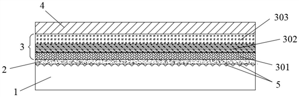
[0035] figure 1It is a structural schematic diagram of a specific embodiment 1 of a high-transmission and shadow-elimination conductive glass of the present invention, from which it can be seen that the present invention provides a high-transmission and shadow-elimination conductive glass, comprising a glass substrate 1 with a thickness of 80nm, on the glass substrate One side of the 1 is etched with several nano-scale anti-reflection holes 5 with tapered structures, the aperture of the nano-scale anti-reflection holes 5 is 3nm, and the porosity is 20%; the glass substrate 1 is etched with nano-scale anti-reflection holes 5 One side is provided with a thickness compensation layer 2 with a thickness of 10 nm. The material of the thickness compensation layer 2 is silicon dioxide, which can not only protect the nanoscale anti-reflection holes 5 to a certain extent, but also protect the upper functional layer, killing two birds with one stone. A transition film layer 3 with a thic...
specific Embodiment 2
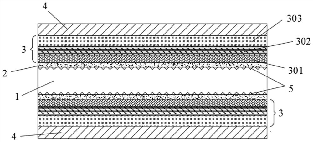
[0047] figure 2 It is a structural schematic diagram of a specific embodiment 2 of a high-transmission and shadow-elimination conductive glass of the present invention, from which it can be seen that the present invention provides a high-transmission and shadow-elimination conductive glass, comprising a glass substrate 1 with a thickness of 150nm, on which the glass substrate The upper and lower sides of 1 are etched with several nano-scale anti-reflection holes 5 with a tapered structure, the diameter of the nano-scale anti-reflection holes 5 is 10 nm, and the porosity is 30%; the glass substrate 1 is etched with nano-scale anti-reflection holes 5 A thickness compensation layer 2 with a thickness of 30nm is provided on one side, and the material of the thickness compensation layer 2 is silicon dioxide, which can not only protect the nanoscale anti-reflection holes 5 to a certain degree, but also protect the upper functional layer. Killing two birds with one stone, the thickn...
specific Embodiment 3
[0059] The present invention provides a high-transmission and shadow-eliminating conductive glass, which comprises a glass substrate 1 with a thickness of 100nm. On one side of the glass substrate 1, several nano-scale anti-reflection holes 5 with tapered structures are etched. The nano-scale anti-reflection holes 5 The pore diameter is 8nm, and the porosity is 25%. A 20nm-thick thickness compensation layer 2 is provided on the side of the glass substrate 1 etched with nanoscale anti-reflection holes 5. The material of the thickness compensation layer 2 is silicon dioxide, both The nano-scale anti-reflection hole 5 can be protected to a certain extent, and the upper functional layer can be protected, killing two birds with one stone. The thickness compensation layer 2 is provided with a transition film layer 3 with a thickness of 130 nm, and the transition film layer 3 is provided with a 60 nm film. thick indium tin oxide film layer 4, and electrode patterns are etched on the i...
PUM
| Property | Measurement | Unit |
|---|---|---|
| Aperture | aaaaa | aaaaa |
| Aperture | aaaaa | aaaaa |
| Aperture | aaaaa | aaaaa |
Abstract
Description
Claims
Application Information