Unbiased enzymatic glucose photoelectrochemical sensing electrode and preparation method thereof

A photoelectrochemical and sensing electrode technology, applied in the field of photoelectrochemistry, can solve the problems of small detectable concentration range, high minimum detection limit, and applied working voltage.

Pending Publication Date: 2022-05-10
SUZHOU UNIV
View PDF0 Cites 0 Cited by
  • Summary
  • Abstract
  • Description
  • Claims
  • Application Information

AI Technical Summary

Problems solved by technology

[0003] The present invention provides a non-bias enzymatic glucose

Method used


Image

  • Unbiased enzymatic glucose photoelectrochemical sensing electrode and preparation method thereof
  • Unbiased enzymatic glucose photoelectrochemical sensing electrode and preparation method thereof
  • Unbiased enzymatic glucose photoelectrochemical sensing electrode and preparation method thereof

Examples


Embodiment 1

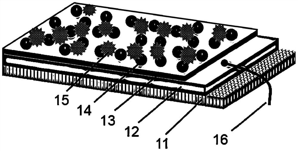
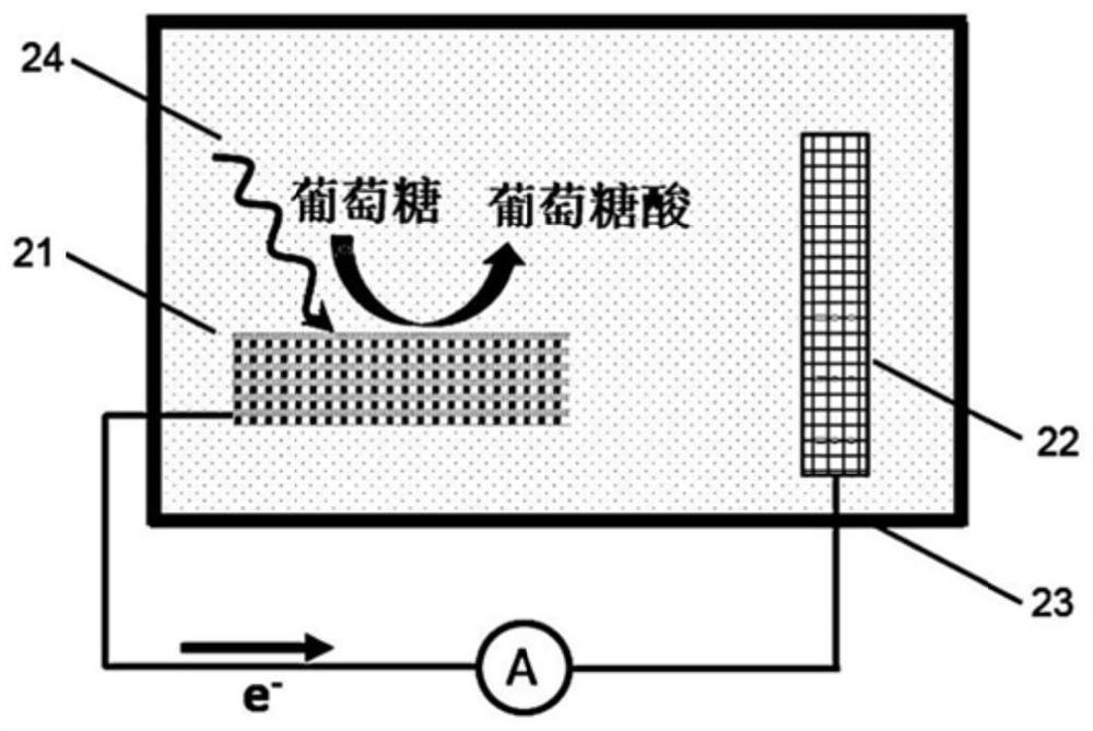
[0040] An unbiased enzymatic glucose photoelectrochemical sensing electrode, such as figure 1 As shown: the glucose photoelectrochemical sensing electrode is a composite structure, which sequentially includes a glucose oxidase layer 15, a metal nanoparticle layer 14, an n-type semiconductor thin film layer 13, a metal thin film layer 12, and a planar insulating layer along the light incident direction. The base 11, and the lead terminal 16 drawn out from the metal film layer. The metal nanoparticle layer 14 forms a Schottky contact with the n-type semiconductor thin film layer 13, so that part of the hot electrons in the metal nanoparticle layer 14 can be collected by the n-type semiconductor thin film layer 13, and at the same time, it can promote the formation of the n-type semiconductor thin film layer. The separation efficiency of the photogenerated electron-hole pair in 13; Described metal film layer 12, n-type semiconductor film layer 13 and metal nanoparticle layer 14 f...

Embodiment 2

[0045] A preparation method of an unbiased enzymatic glucose photoelectrochemical sensing electrode, using planar silicon dioxide (SiO 2 ) as the basis, including:

[0046] 1) After the substrate is chemically cleaned, a 150nm thick aluminum (Al) film is deposited on its surface by DC magnetron sputtering;

[0047] 2) A layer of 180 nm thick titanium dioxide (TiO 2 )film;

[0048] 3) Heat treatment at 500°C for 2 hours in an air atmosphere;

[0049] 4) Obtain a layer of gold nanoparticles (Au NPs) by light-assisted electrochemical deposition;

[0050] 5) Oxygen plasma treatment to increase the hydrophilicity of the composite structure of the titanium dioxide film layer and the gold nanoparticle layer;

[0051] 6) modifying the glucose oxidase (GOx) layer on the surface of the composite structure of the titanium dioxide film layer and the gold nanoparticle layer by a spin coating method;

[0052] 7) Dry naturally to get SiO 2 / Al / TiO 2 / Au NPs / GOx stacked structure;

[...


PUM

PropertyMeasurementUnit
Diameteraaaaaaaaaa
Thicknessaaaaaaaaaa
Thicknessaaaaaaaaaa

Abstract

The invention belongs to the field of photoelectrochemistry, and discloses a bias-voltage-free enzymatic glucose photoelectrochemical sensing electrode and a preparation method thereof.The bias-voltage-free enzymatic glucose photoelectrochemical sensing electrode sequentially comprises a glucose oxidase layer, a metal nanoparticle layer, an n-type semiconductor thin film layer, a metal thin film layer and a plane insulation substrate in the light incidence direction; the metal film layer and the n-type semiconductor film layer form ohmic contact; the metal nanoparticle layer and the n-type semiconductor thin film layer form Schottky contact; and an optical resonant cavity is formed among the metal film layer, the n-type semiconductor film layer and the metal nanoparticle layer. When a light source irradiates the sensing electrode, the metal nanoparticle layer and the n-type semiconductor film layer can generate effective light absorption and generate a hot electron hole pair and a photo-induced electron hole pair respectively; under the action of the Schottky junction, the hot holes and the photo-generated holes are transferred to glucose molecules under the catalytic action of glucolase; and the glucose concentration is detected by monitoring the change of the light current.

Description

technical field [0001] The invention belongs to the field of photoelectrochemistry, and relates to a photoelectrochemical sensing electrode for glucose and a preparation method thereof. Background technique [0002] Diabetes is a common disease, and detecting glucose content in blood and urine is an indispensable means for diagnosing diabetes. The main detection methods of glucose are spectrometry, mass spectrometry, electrochemical method and photoelectrochemical method. Among them, photoelectrochemical sensing is a detection method developed in recent years. A photoelectrochemical sensor is a device that analyzes a target based on the photoelectrochemical response of a photoelectrode. When effective light is introduced, the photoelectrode absorbs photons to form photogenerated electrons and holes, and the photogenerated electrons and holes participate in the chemical generation of the target or other substances in the background liquid, causing changes in photocurrent or...

Claims


Application Information

Patent Timeline
IPC IPC(8): G01N27/327G01N27/30
CPCG01N27/3272G01N27/3278G01N27/305
Inventor 吴绍龙于逸凡马露秦琳玲卢文祥李孝峰
Owner SUZHOU UNIV
Why Eureka
Try Eureka