

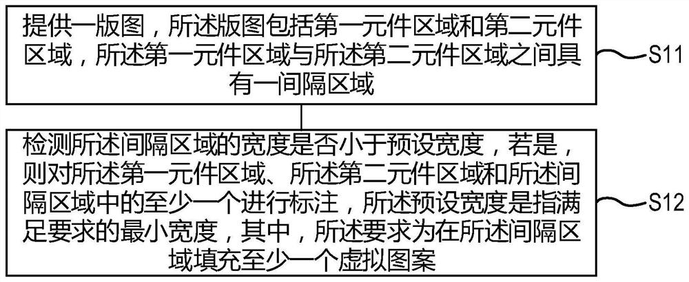
Integrated circuit layout method and layout device
An integrated circuit and layout technology, applied in the direction of circuits, CAD circuit design, electrical components, etc., can solve the problems of low layout efficiency of integrated circuits, improve layout accuracy, improve lithography quality, and improve layout efficiency Effect
- Summary
- Abstract
- Description
- Claims
- Application Information
AI Technical Summary
Problems solved by technology
Method used
Image

Examples
Embodiment Construction
[0062] The specific embodiments of the layout method and the layout device of the integrated circuit provided by the present invention will be described in detail below with reference to the accompanying drawings.
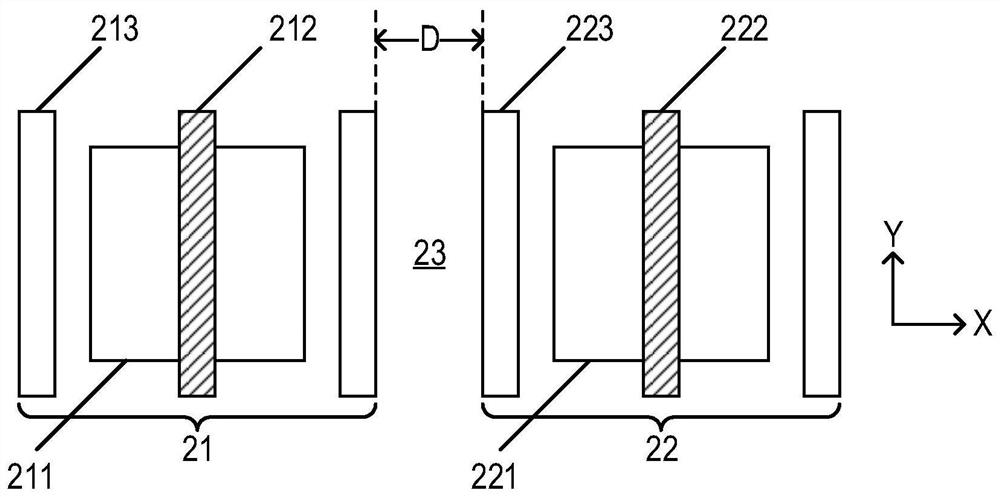
[0063] This specific embodiment provides a layout method of an integrated circuit, with the attached figure 1 It is a flow chart of the layout method of the integrated circuit in the specific embodiment of the present invention, with the attached Figures 2A-2D It is a schematic diagram of detecting a layout in the specific embodiment of the present invention. like figure 1 , Figures 2A-2D As shown, the layout method of an integrated circuit provided by this specific embodiment includes the following steps:
[0064] Step S11, providing a layout, the layout includes a first component area 21 and a second component area 22, and there is an interval area 23 between the first component area 21 and the second component area 22, such as Figure 2A shown.
[0065] S...
PUM
 Abstract
Description
Claims
Application Information