Printing preparation method and application of single-orientation organic semiconductor crystal patterned array

A technology of organic semiconductors and crystal patterns, applied in semiconductor/solid-state device manufacturing, semiconductor devices, replication/marking methods, etc., can solve the problem of precise control of patterned arrays that are difficult to single orientation

Pending Publication Date: 2022-05-10
INST OF CHEM CHINESE ACAD OF SCI
View PDF4 Cites 0 Cited by
  • Summary
  • Abstract
  • Description
  • Claims
  • Application Information

AI Technical Summary

Problems solved by technology

[0005] Aiming at the problem that it is difficult to realize the precise control of single-orientation patterned arrays in the preparation of organic semiconductor crystals in the prior art, the present invention provides a printing preparation method for single-orientation organic semiconductor crystal patterned arrays, and the prepared organic semiconductor crystal pattern The high-quality crystallization and highly consistent orientation of the crystallization array can significantly improve the performance of the device

Method used


Image

  • Printing preparation method and application of single-orientation organic semiconductor crystal patterned array
  • Printing preparation method and application of single-orientation organic semiconductor crystal patterned array
  • Printing preparation method and application of single-orientation organic semiconductor crystal patterned array

Examples


Embodiment 1

[0049] (1) Preparation of pretreatment patterned substrate material

[0050] SiO 2 / Si wafers were ultrasonically cleaned and dried with water, acetone, isopropanol, etc., and lyophilized with phenyltrichlorosilane. The treatment conditions were: vacuum, 4 hours, and 85°C to obtain the isopropylsilyne Lyophilic SiO with static contact angle of 2° in o-dichlorobenzene solution of pentacene (TIPS-PEN) 2 / Si base material.

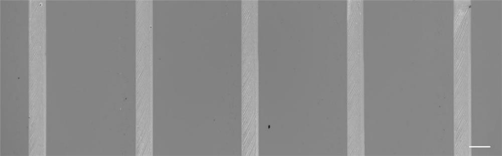
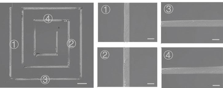
[0051] The resulting lyophilic SiO 2 Spin-coat a layer of photoresist (SU-8) on the / Si base material, and with the help of a mask, irradiate the surface of the base material with a photoresist film with ultraviolet light, causing a chemical reaction of the photoresist in the exposed area; Then, the photoresist in the unexposed area is dissolved and removed by infiltration and development technology, so that the pattern on the mask plate is copied to the photoresist film, and the SiO with the patterned photoresist is obtained. 2 / Si base material.

[005...

Embodiment 2

[0058] (1) Preparation of pretreated substrate

[0059] SiO 2 / Si wafers were ultrasonically cleaned and dried with water, acetone, isopropanol, etc., and lyophilized with phenyltrichlorosilane. The treatment conditions were: vacuum, 5 h, and 100 °C to obtain the 2,7-bis Octyl[1]benzothieno[3,2-B]benzothiophene (C 8 Lyophilic SiO with a static contact angle of 5° in chlorobenzene solution of -BTBT) 2 / Si base material.

[0060] The resulting lyophilic SiO 2 / Si base material is spin-coated with a layer of photoresist (Z520), and with the help of a mask, the SiO with photoresist film is irradiated with ultraviolet light. 2 / Si base material surface, causing the photoresist in the exposed area to undergo a chemical reaction; then the photoresist in the unexposed area is dissolved and removed by infiltration and development technology, so that the pattern on the mask plate is copied to the photoresist film, and the band is obtained. SiO with photoresist patterning 2 / Si bas...

Embodiment 3

[0067] (1) Preparation of pretreated substrate

[0068] SiO 2 / Si wafers were ultrasonically cleaned and dried with water, acetone, isopropanol, etc., and lyophilized with phenyltrichlorosilane. The treatment conditions were: vacuum, 2 hours, and 65°C. Lyophilic SiO with a static contact angle of 30° in ether solution 2 / Si base material.

[0069] The resulting lyophilic SiO 2 / Si base material is spin-coated with a layer of photoresist (HSQXR-1541-006), and with the help of a mask, irradiate the SiO with photoresist film with ultraviolet light 2 / Si base material surface, causing the photoresist in the exposed area to undergo a chemical reaction; then the photoresist in the unexposed area is dissolved and removed by infiltration and development technology, so that the pattern on the mask plate is copied to the photoresist film, and the band is obtained. SiO with photoresist patterning 2 / Si base material.

[0070] The SiO with photoresist pattern 2 The / Si substrate ma...


PUM

PropertyMeasurementUnit
thicknessaaaaaaaaaa
thicknessaaaaaaaaaa

Abstract

The invention relates to the field of organic semiconductor crystal printing, and discloses a printing preparation method and application of a single-orientation organic semiconductor crystal patterned array. The preparation method of the organic semiconductor crystal array comprises the following steps: pre-treating a substrate material and printing an organic semiconductor functional material on the pre-treated substrate material. According to the single-orientation organic semiconductor crystal patterned array disclosed by the invention, the patterned design of a heterogeneous wettability base material and the regulation and control of the adhesive force characteristic of an organic functional material are utilized to induce the micro-area deformation of a micron-sized meniscus solid-liquid-gas three-phase line (TCL), so that the crystallization behaviors of nucleation, growth and the like of organic molecules are precisely regulated and controlled; and finally, the preparation of the controllable orientation organic semiconductor crystal patterned array on any base material is realized. The performance of the single-orientation organic semiconductor crystal patterned device is three times that of a multi-orientation crystal device, and the single-orientation organic semiconductor crystal patterned device is expected to be applied to organic high-performance integrated devices.

Description

technical field [0001] The invention relates to the field of organic semiconductor crystal printing, in particular to a printing preparation method and application of a controllable single-orientation organic semiconductor crystal patterned array. Background technique [0002] Organic semiconductor crystals have been applied in many electronic and optoelectronic devices, such as organic field-effect transistors (OFETs), organic light-emitting diodes (OLEDs), and photovoltaic cells (OPVs), due to their inherent long-range order, absence of grain boundaries, and low defect density. Organic semiconductor crystals with precisely controlled orientation are of great significance for the integration of high-performance devices. Carrier transport in organic single crystals is anisotropic, and uniform and controllable orientation is conducive to achieving the best charge transport performance, and can also avoid device-to-device variability and achieve low crosstalk in integrated dev...

Claims


Application Information

Patent Timeline
Patent Type & Authority Applications(China)
IPC IPC(8): H01L51/56H01L51/48H01L51/40H01L51/54H01L51/46H01L51/30B41J3/407B41J3/413B41M5/00G03F7/16G03F7/42
CPCB41M5/0041B41J3/413B41J3/4073B41J3/407B41M5/0058B41M5/007G03F7/162G03F7/422G03F7/428H10K71/13H10K71/12H10K85/111H10K85/113H10K85/623H10K85/622H10K85/655Y02E10/549
Inventor 乔雅丽陈胜楠宋延林
Owner INST OF CHEM CHINESE ACAD OF SCI
Why Eureka
Try Eureka