N-surface GaN-based p-channel device for improving ohmic contact resistance and preparation method of N-surface GaN-based p-channel device

A technology of ohmic contact and channel devices, applied in semiconductor/solid-state device manufacturing, electrical components, semiconductor devices, etc., can solve the problem of deteriorating the electrical characteristics of P-channel devices, reducing GaN hole mobility, and affecting the characteristics of P-channel devices and other problems, to increase the hole tunneling probability, reduce the barrier thickness, and improve the effect of ohmic contact characteristics

Pending Publication Date: 2022-05-24
XIDIAN UNIV
View PDF0 Cites 0 Cited by
  • Summary
  • Abstract
  • Description
  • Claims
  • Application Information

AI Technical Summary

Problems solved by technology

The lower hole concentration makes the ohmic contact properties prepared on this P-GaN poor, which in turn affects the characteristics of P-channel devices
In addition, the additional interface charge brought by the deposition of the insulating layer dielectric under the gate further reduces the hole mobility in GaN, and these problems greatly deteriorate the electrical characteristics of the P-channel device.

Method used


Image

  • N-surface GaN-based p-channel device for improving ohmic contact resistance and preparation method of N-surface GaN-based p-channel device
  • N-surface GaN-based p-channel device for improving ohmic contact resistance and preparation method of N-surface GaN-based p-channel device
  • N-surface GaN-based p-channel device for improving ohmic contact resistance and preparation method of N-surface GaN-based p-channel device

Examples


Embodiment 1

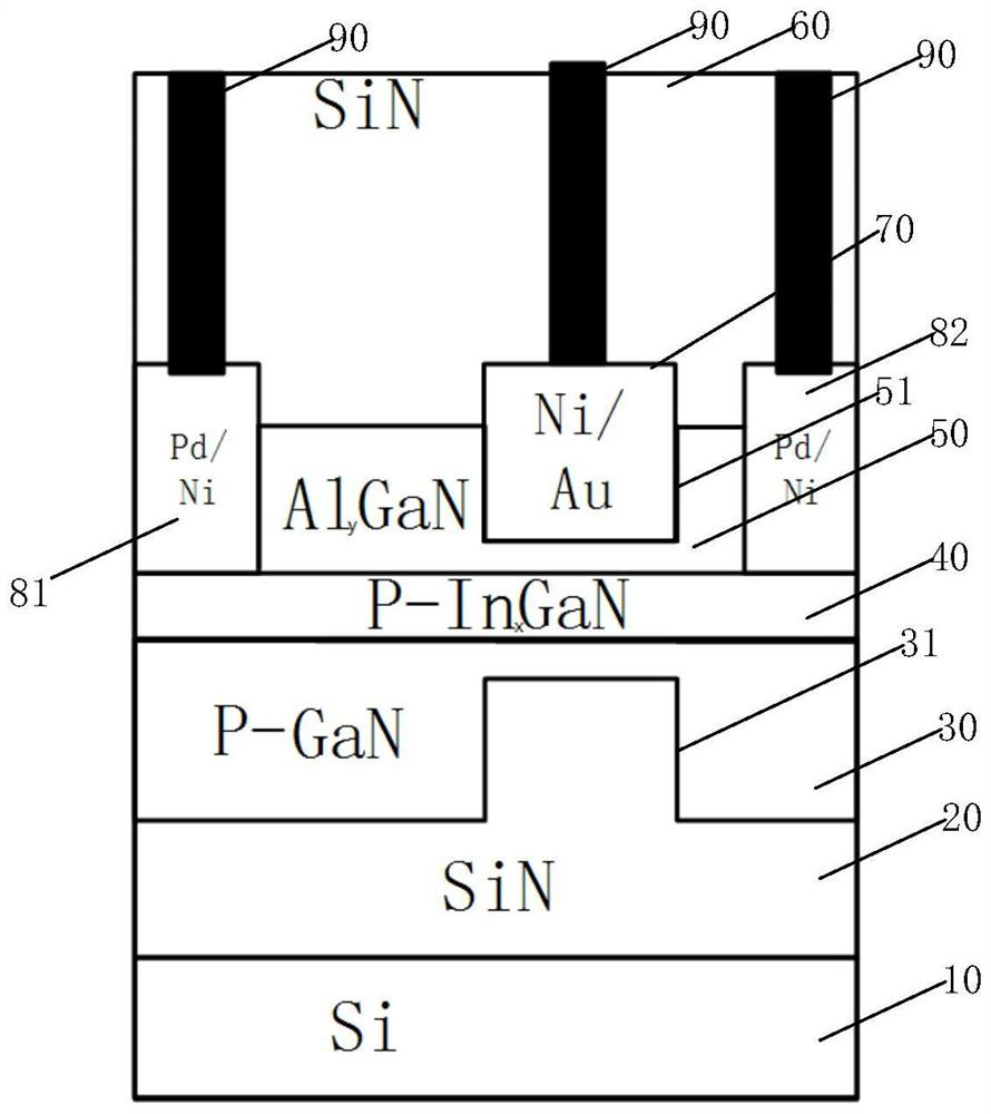
[0068] See figure 1 , an embodiment of the present invention provides an N-face GaN-based P-channel device with improved ohmic contact resistance, comprising: a first Si substrate layer 10, a first protective layer 20, a P-GaN layer 30, a P-GaN layer 30, a -In x GaN layer 40, Al y The GaN barrier layer 50 and the second protective layer 60 .

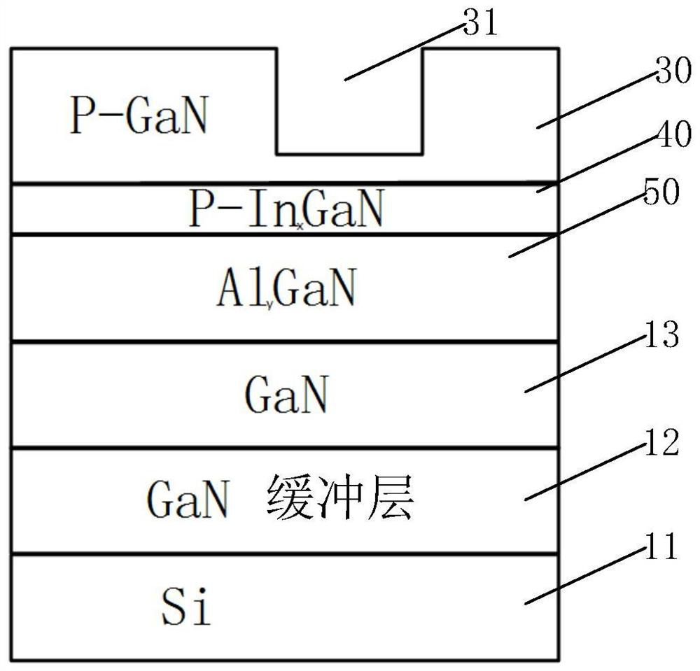
[0069] Al y GaN barrier layer 50, P-In x The GaN layer 40 and the P-GaN layer 30 form an N-plane heterojunction structure. A first groove 31 is formed on the P-GaN layer 30 . The notch of the first groove 31 faces the first protective layer 20 , and the first groove 31 is filled with the first protective layer 20 .

[0070] P-In x The Mg doping concentration of the GaN layer 40 is 2e19 / cm 3 ~3e19 / cm 3 , the thickness is 10nm ~ 20nm. Among them, 0.05≤x≤0.1.

[0071] Al y A second groove 51 opposite to the first groove 31 is formed on the GaN barrier layer 50 . Al y A source electrode 81 and a drain electrode 82 are deposited...

Embodiment 2

[0079] A second aspect of the embodiment of the present invention provides a method for preparing an N-face GaN-based P-channel device with improved ohmic contact resistance, which is used to prepare the device in the first embodiment, including the following steps:

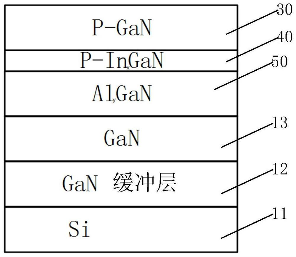
[0080] Step 1. Epitaxially growing materials on the second Si substrate layer 11, the epitaxial layers are respectively the GaN buffer layer 12, the GaN layer 13, the Al from bottom to top y GaN barrier layer 50, P-In x GaN layer 40 and P-GaN layer 30; wherein, P-In x The Mg doping concentration of the GaN layer 40 is 2e19 / cm 3 ~3e19 / cm 3 , the thickness is 10nm ~ 20nm.

[0081] Step 2: Etching the first groove 31 on the P-GaN layer 30 .

[0082] Step 3, depositing the first protective layer 20 on the surface of the P-GaN layer 30 and filling the first groove 31 .

[0083] Step 4, bonding the first Si substrate layer 10 on the surface of the first protective layer 20 .

[0084] Step 5, turn over the product...

Embodiment 3

[0094] The embodiment of the present invention provides a method for preparing an N-face GaN-based P-channel device with improved ohmic contact resistance, which is used to prepare the device in the first embodiment, including the following steps:

[0095] Step 301, using the MOCVD method to epitaxially grow the material on the second Si substrate layer 11, the epitaxial layers from bottom to top are the GaN buffer layer 12, the GaN layer 13, the Al y GaN barrier layer 50, P-In x GaN layer 40 and P-GaN layer 30; wherein, P-In x The Mg doping concentration of the GaN layer 40 is 2e19 / cm 3 ~3e19 / cm 3 , the thickness is 10nm ~ 20nm. like Figure 2a shown.

[0096] The thickness of the GaN buffer layer 12 is 2 μm to 5 μm. The thickness of the GaN layer 13 is 100 nm to 200 nm. Al y The thickness of the GaN barrier layer 50 is 15 nm to 25 nm. The thickness of the P-GaN layer 30 is 30 to 50 nm. The doping concentration of Mg in the P-GaN layer 30 is 2e19 / cm 3 ~3e19 / cm 3 ....


PUM

PropertyMeasurementUnit
thicknessaaaaaaaaaa
thicknessaaaaaaaaaa
depthaaaaaaaaaa

Abstract

The invention discloses an N-face GaN-based P-channel device for improving ohmic contact resistance and a preparation method thereof. The N-face GaN-based P-channel device comprises a first Si substrate layer, a first protection layer, a P-GaN layer, a P-InxGaN layer, an AlyGaN barrier layer and a second protection layer which are sequentially arranged from bottom to top. The AlyGaN barrier layer, the P-InxGaN layer and the P-GaN layer form a heterojunction structure of an N surface; the thickness of the P-In < x > GaN layer ranges from 10 nm to 20 nm. Wherein x is not less than 0.05 and not more than 0.1; a second groove opposite to the first groove is formed in the AlyGaN barrier layer; a source electrode and a drain electrode are respectively deposited on two sides of the AlyGaN barrier layer; wherein y is greater than or equal to 0.2 and less than or equal to 0.3; a gate electrode is arranged on the second groove; interconnection metal penetrating through the second protection layer is deposited above the source electrode, the drain electrode and the gate electrode respectively. According to the P-channel device prepared by using the N-surface heterojunction material, the influence of interface charges introduced by an under-gate deposition insulating medium under the condition of a Ga surface on the hole mobility can be avoided, the reduction of the hole mobility is avoided, and the ohmic contact characteristic of the device is improved, so that the performance of the device is improved.

Description

technical field [0001] The invention belongs to the technical field of semiconductor devices, and in particular relates to an N-face GaN-based P-channel device with improved ohmic contact resistance and a preparation method thereof. Background technique [0002] GaN is the primary choice for next-generation high-frequency high-power devices and power electronics due to its excellent material properties. With the increase in application requirements for devices such as power switches, additional parasitic effects brought about by using Si-based CMOS devices to drive devices such as GaN power switches affect the performance of the device. Therefore, it is particularly important to fabricate GaN-based CMOS devices on the same wafer as GaN-based power switches and other devices. As an important part of GaN-based CMOS devices, GaN-based P-channel devices have been paid attention to and a lot of research has been started. The actual hole concentration in the grown P-GaN layer (3...

Claims


Application Information

Patent Timeline
Patent Type & Authority Applications(China)
IPC IPC(8): H01L29/45H01L29/778H01L21/335
CPCH01L29/452H01L29/778H01L29/66462Y02P70/50
Inventor 马晓华王博麟张濛牛雪锐杨凌侯斌武玫宓珉瀚郝跃
Owner XIDIAN UNIV
Why Eureka
Try Eureka