Laminated structure and semiconductor device

A structure and semiconductor technology, applied in the fields of semiconductor devices, semiconductor/solid-state device manufacturing, semiconductor/solid-state device components, etc., can solve the problems that are still in progress, and achieve excellent heat dissipation, good film thickness distribution, and large area. Effect

Pending Publication Date: 2022-05-27
FLOSFIA
View PDF11 Cites 0 Cited by
  • Summary
  • Abstract
  • Description
  • Claims
  • Application Information

AI Technical Summary

Problems solved by technology

[0006] In addition, patent documents 1 to 11 are related publications of the applicant's patent or patent application, and the current research is still in progress

Method used


Image

  • Laminated structure and semiconductor device
  • Laminated structure and semiconductor device
  • Laminated structure and semiconductor device

Examples


Embodiment

[0151] Embodiments of the present invention will be described below using the accompanying drawings, but the present invention is not limited thereto.

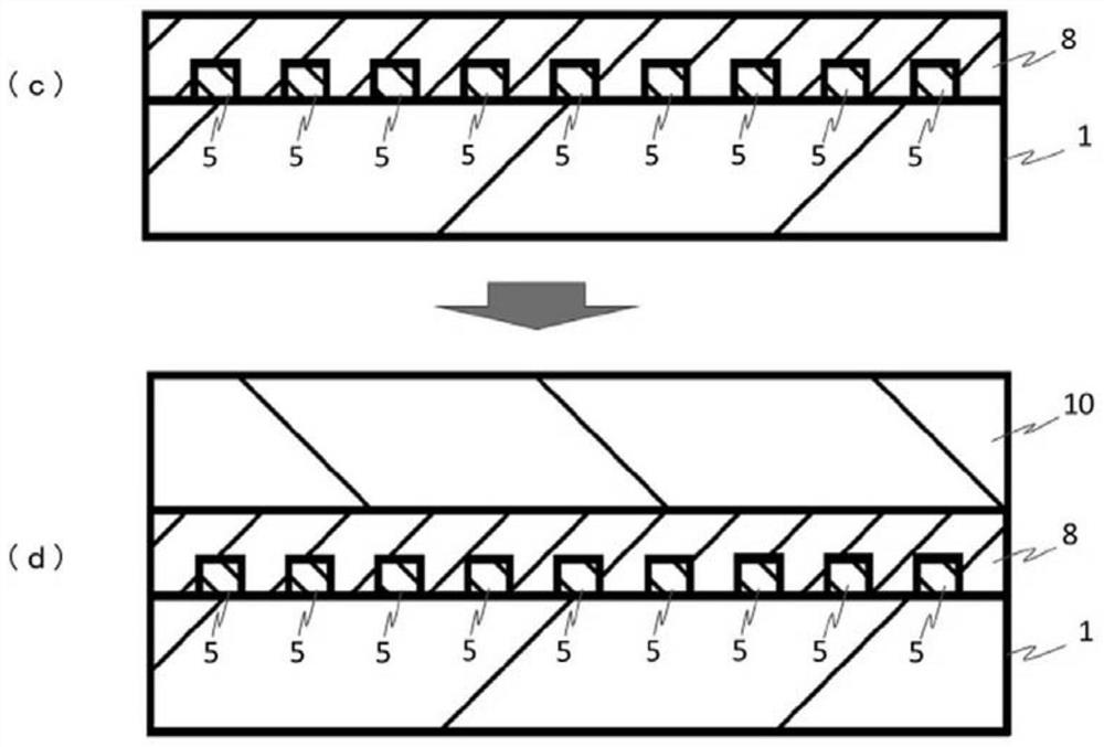
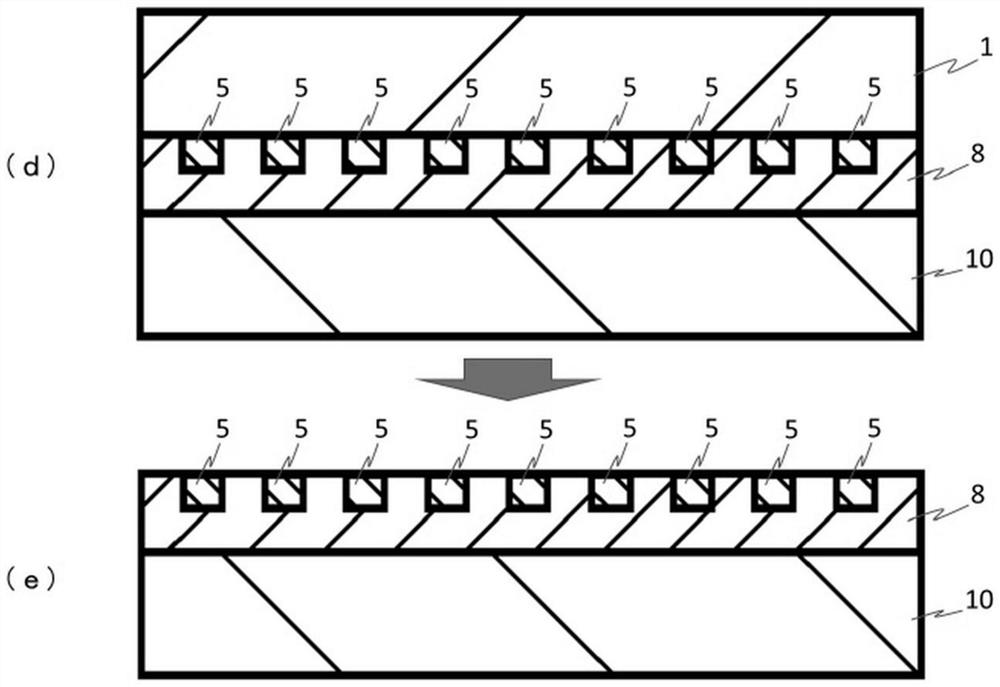
[0152] The laminated structure can be obtained by a method in which a crystal growth layer is formed on a substrate for crystal growth by crystal growth including lateral crystal growth, and a support having a thermal conductivity of 100 W / m·k or more at room temperature is attached to the substrate. On the crystal growth layer, the substrate for crystal growth is subsequently peeled off, whereby the laminated structure can be obtained.

[0153] (Example)

[0154] 1. Fabrication of laminated structure

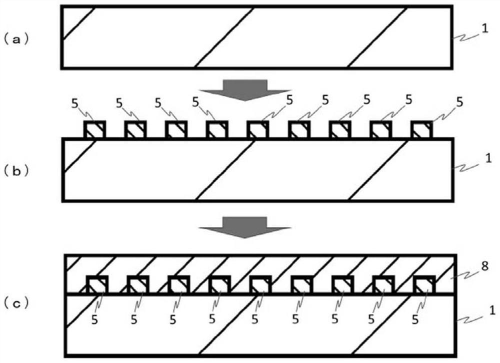
[0155] As a substrate for crystal growth, an ELO mask is formed on the surface. In addition, a sapphire substrate was used as a substrate for crystal growth. In the present invention, as the sapphire substrate, a sapphire substrate having an r-plane or an S-plane as a main surface is preferably used. figure 1 (a) shows the ...


PUM

PropertyMeasurementUnit
thicknessaaaaaaaaaa
areaaaaaaaaaaa
areaaaaaaaaaaa

Abstract

Provided is a laminated structure which is useful for a semiconductor device, has a crystalline film having a large area, a good film thickness distribution, and a film thickness of 30 [mu] m or less, and has excellent heat dissipation properties. The present invention relates to a laminated structure in which a crystalline film containing a crystalline metal oxide as a main component is laminated on a support directly or via another layer, the support having a thermal conductivity of 100 W / m.K or more at room temperature, the crystalline film having a corundum structure, the film thickness of the crystalline film being 1-30 [mu] m, and the thickness of the crystalline film being 1-30 [mu] m. The crystalline film has an area of 15 cm2 or more, and the distribution of the film thickness in the area is within the range of + / -10% or less.

Description

technical field [0001] The present invention relates to a laminated structure useful for semiconductor devices. Background technique [0002] Gallium oxide (Ga 2 O 3 ) semiconductor devices are attracting attention, and it is expected that they can be applied to power semiconductor devices such as inverters. In addition, it is expected to be widely used in light receiving / emitting devices such as LEDs and sensors because of the wide band gap. In particular, α-Ga having a corundum structure in gallium oxide 2 O 3 etc., according to Non-Patent Document 1, the band gap can be controlled by forming a mixed crystal with indium or aluminum, respectively, or by forming a mixed crystal in combination with them, which constitutes a very attractive material system as an InAlGaO-based semiconductor. Here the InAlGaO-based semiconductor is composed of In X Al Y Ga Z O 3 (0≦X≦2, 0≦Y≦2, 0≦Z≦2, X+Y+Z=1.5 to 2.5) represents (Patent Document 9, etc.), and can be viewed as the same m...

Claims


Application Information

Patent Timeline
Patent Type & Authority Applications(China)
IPC IPC(8): H01L29/04H01L29/24H01L23/373H01L21/02H01L21/34H01L21/683
CPCH01L29/24H01L23/3738H01L29/045H01L29/04H01L21/34H01L21/02565H01L21/6835H01L2221/6835C23C16/40C30B25/18C30B29/16C30B33/06H01L29/739H01L29/78H01L29/861H01L29/868H01L29/872C30B25/04H01L21/02647H01L21/0242H01L21/02414H01L21/02433H01L21/02483H01L21/0262H01L21/02628H01L23/373H01L23/3736H01L23/4334H01L23/42H01L21/4871C03B33/06H01L29/772H01L21/20H01L29/12H01L29/4925
Inventor 大岛孝仁鸟山达矢
Owner FLOSFIA
Why Eureka
Try Eureka