
Method for drawing six-inch zone-melting silicon single crystal and used heat shield

A technology for zone melting of silicon and silicon single crystal, applied in the field of semiconductor silicon single crystal growth, can solve the problems of single crystal transformation, single crystal burst or crystal transformation, dislocation, etc.

Pending Publication Date: 2022-06-03
CHINA ELECTRONICS TECH GRP NO 46 RES INST
View PDF0 Cites 0 Cited by
  • Summary
  • Abstract
  • Description
  • Claims
  • Application Information

AI Technical Summary

Problems solved by technology

When the cooling rate is too high, the temperature gradient inside and outside the single crystal is too large, causing the single crystal to burst and crystallization to fail; when the cooling rate is too small, the melt cannot solidify in time, resulting in remelting, resulting in single crystal crystallization and crystallization fail
The large-size area of ​​molten silicon single crystal growth, the edge heat dissipation is faster, the center heat dissipation is slower, the edge solidifies before the center, and when the center solidifies later, volume expansion will occur and internal stress will occur. When the expansion reaches a certain level, the generated stress will reach At the limit, the single crystal will burst or crystallize, and a large number of dislocations will be generated, which will lead to the failure of crystal formation

Method used


Image

  • Method for drawing six-inch zone-melting silicon single crystal and used heat shield
  • Method for drawing six-inch zone-melting silicon single crystal and used heat shield

Examples


Embodiment Construction

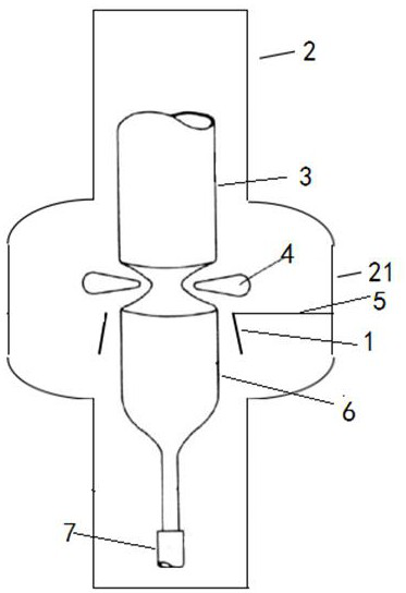
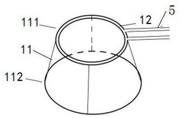
[0013] like figure 2 As shown in the figure, a heat shield for drawing a fused silicon single crystal in a six-inch area includes a heat shield cover 11 and a condensation pipeline 12. The heat shield cover 11 is a copper plate conical cover transparent from top to bottom, and the condensation pipeline 12 is selected from The copper pipes are arranged spirally along the upper edge 111 of the entire heat shield 11, and the copper pipes 5 at both ends of the condensation pipe 12 are drawn out to form the outlet end and the inlet end of the cooling water.

[0014] like figure 1 , figure 2 As shown, a method for pulling a six-inch zone molten silicon single crystal includes the processes of evacuation, preheating, compounding, neck narrowing, shoulder expansion, shoulder turning, equal diameter, finishing, furnace shutdown, and furnace disassembly and assembly; Before evacuation, first enclose the copper tube of the condensation pipeline 12 into a ring with a diameter of 190mm...


PUM


Abstract

The invention relates to a method for drawing a six-inch zone-melting silicon single crystal and a heat shield used in the method. A heat shield is arranged at a position 40mm below a heating coil in a middle furnace chamber of the zone-melting single crystal furnace, the diameter of the upper edge of the heat shield is 90mm, the diameter of the lower edge of the heat shield is 215mm, the height of the heat shield is 40mm, and the pressure of cooling water in a condensation pipeline is 3.2 bar; when the procedures of shoulder expansion, shoulder rotation, equal diameter and ending are carried out, the silicon single crystal moves downwards along with the lower shaft and enters the heat shield area, heat reflected by the heat shield acts on the lower portion of the silicon single crystal, and the phenomenon that due to the fact that the temperature gradient is too large or too small, the silicon single crystal explodes or melts back, and crystal forming fails is avoided.

Description

technical field [0001] The invention relates to the technical field of semiconductor silicon single crystal growth, in particular to a method for pulling a six-inch zone fused silicon single crystal and a heat shield used. Background technique [0002] District fused silicon single crystal has the irreplaceable advantages of high purity, high resistivity and low oxygen and carbon content, which cannot be replaced by Czochralski silicon single crystal. An indispensable material for power devices. [0003] Wacker of Germany, Shin-Etsu, Sumco and other foreign melters have already grown large-size dislocation-free silicon fused monocrystals, which have imposed a technological blockade on my country and have taken a monopoly in the regional fused silicon single crystal market. In recent years, the diameter of the single crystal silicon market has gradually moved towards a large size, and the trend of large size of the area fused silicon single crystal has become imperative. Ho...

Claims


Application Information

Patent Timeline
IPC IPC(8): C30B13/00C30B29/06
CPCC30B13/00C30B29/06Y02P40/57
Inventor 李明佳李聪张瀚文冯旭郑万超刘洪张伟才
Owner CHINA ELECTRONICS TECH GRP NO 46 RES INST
Learn More