Free layer of MRAM (Magnetic Random Access Memory), preparation method of free layer and magnetic tunnel junction of MRAM
A free, magnetic layer technology, applied in the field of magnetoresistive devices, can solve the problems of reducing the thickness of the magnetic film, Hk reduction, etc., to reduce the interface damage, improve the vertical magnetic anisotropy field, and improve the data retention ability.
- Summary
- Abstract
- Description
- Claims
- Application Information
AI Technical Summary
Problems solved by technology
Method used
Image
Examples
preparation example Construction
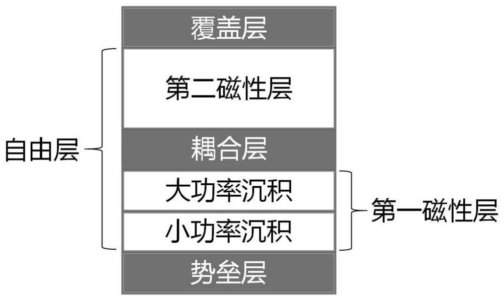
[0041] The present invention also provides a preparation method of the free layer described in the above technical solution, comprising the following steps:
[0042] Using magnetron sputtering technology, several layers of magnetic layers and coupling layers are alternately deposited on the barrier layer to form a free layer;
[0043] Wherein, the magnetic layer in contact with the potential barrier layer is deposited and formed under at least two different magnetron sputtering powers, and the magnetron sputtering power on the side near the potential barrier layer is the smallest.
[0044] In the preparation method provided by the present invention, the free layer structure is prepared by layer-by-layer deposition on the barrier layer. Wherein, the deposition method is magnetron sputtering, the magnetic layer in contact with the barrier layer is deposited and formed under at least two different magnetron sputtering powers, and the magnetron sputtering power on the side near th...
Embodiment 1
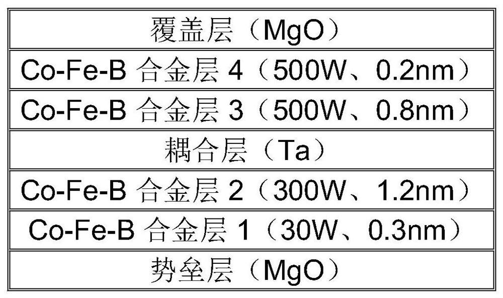
[0049] Using magnetron sputtering technology, deposit Co-Fe-B alloy layer 1, Co-Fe-B alloy layer 2, coupling layer, Co-Fe-B alloy layer 3, Co-Fe-B alloy layer on the barrier layer in sequence Layer 4 and overlay.
[0050] Among them, the material of the barrier layer is MgO, the thickness is 2nm, the deposition power of the Co-Fe-B alloy layer 1 is 30W, the deposition thickness is 0.3nm, the deposition power of the Co-Fe-B alloy layer 2 is 300W, and the deposition thickness is 300W. is 1.2nm, the material of the coupling layer is Ta, the thickness is 0.4nm, the deposition power of Co-Fe-B alloy layer 3 is 500W, the deposition thickness is 0.8nm, the deposition power of Co-Fe-B alloy layer 4 is 500W, The deposition thickness is 0.2 nm, and the material of the cover layer is MgO with a thickness of 1.0 nm. The final free layer structure is as figure 2 shown, figure 2 It is a schematic diagram of the structure of the free layer provided in Embodiment 1 of the present inventi...
Embodiment 2
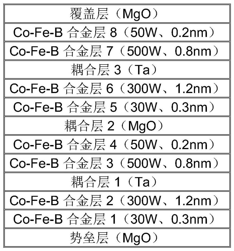
[0061] Using magnetron sputtering technology, deposit Co-Fe-B alloy layer 1, Co-Fe-B alloy layer 2, coupling layer 1, Co-Fe-B alloy layer 3, Co-Fe-B on the barrier layer in sequence Alloy layer 4, coupling layer 2, Co-Fe-B alloy layer 5, Co-Fe-B alloy layer 6, coupling layer 3, Co-Fe-B alloy layer 7, Co-Fe-B alloy layer 8 and cover layer .
[0062] Among them, the material of the barrier layer is MgO, the thickness is 2.0nm, the deposition power of the Co-Fe-B alloy layer 1 is 30W, the deposition thickness is 0.3nm, the deposition power of the Co-Fe-B alloy layer 2 is 300W, and the deposition power is 300W. The thickness is 1.2nm, the material of coupling layer 1 is Ta, the thickness is 0.3nm, the deposition power of Co-Fe-B alloy layer 3 is 500W, the deposition thickness is 0.8nm, and the deposition power of Co-Fe-B alloy layer 4 is 50W, the deposition thickness is 0.2nm, the material of the coupling layer 2 is MgO, the thickness is 0.7nm, the deposition power of the Co-Fe-B...
PUM
| Property | Measurement | Unit |
|---|---|---|
| Thickness | aaaaa | aaaaa |
| Thickness | aaaaa | aaaaa |
| Thickness | aaaaa | aaaaa |
Abstract
Description
Claims
Application Information
 - Generate Ideas
- Intellectual Property
- Life Sciences
- Materials
- Tech Scout
- Unparalleled Data Quality
- Higher Quality Content
- 60% Fewer Hallucinations
Browse by: Latest US Patents, China's latest patents, Technical Efficacy Thesaurus, Application Domain, Technology Topic, Popular Technical Reports.
© 2025 PatSnap. All rights reserved.Legal|Privacy policy|Modern Slavery Act Transparency Statement|Sitemap|About US| Contact US: help@patsnap.com


