Electromagnetic shielding packaging body and preparation method thereof

An electromagnetic shielding and encapsulation technology, applied in the field of electromagnetic shielding encapsulation and its preparation, can solve the problems of complex circuit board structure, poor shielding effect, short circuit of shielding film, etc., to ensure electromagnetic shielding effect, improve grounding reliability, prevent The effect of direct contact

Pending Publication Date: 2022-07-05
SHENZHEN JOHAN MATERIAL TECH CO LTD +1
View PDF4 Cites 0 Cited by
  • Summary
  • Abstract
  • Description
  • Claims
  • Application Information

AI Technical Summary

Problems solved by technology

Due to the complex structure of the circuit board, the spraying technology needs to do complex masking treatment, and the sprayed paste is easy to accumulate between the narrow-pitch electronic components, which increases the weight of the circuit board. Therefore, the spraying conformal technology is difficult to adapt to high-density integrated circuits. plate
For the film-covered conformal technology, when the integration degree of the circuit board i

Method used


Image

  • Electromagnetic shielding packaging body and preparation method thereof
  • Electromagnetic shielding packaging body and preparation method thereof
  • Electromagnetic shielding packaging body and preparation method thereof

Examples


Embodiment 1

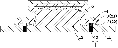
[0086] This embodiment proposes an electromagnetic shielding package and a preparation method thereof. The electromagnetic shielding package includes an integrated circuit board 1 , an insulating film 2 , a shielding film 4 and a protective film 5 , and the upper end of the grounding terminal 13 is exposed on the substrate 11 . Side (structure can refer to appendix figure 2 , 3 shown), and the groove 21 is arranged in a closed ring around the outer periphery of the electronic component 12 , and the conductive portion 3 is a plurality of sections of conductive glue arranged at discontinuous intervals along the extending direction of the groove 21 . Specifically, two electronic components 12 are provided on the substrate 11 , the minimum distance between the two electronic components 12 is 0.5 mm, and the width of the ground terminal 13 is 1.0 mm. The composition of insulating film 2 includes aluminum oxide and epoxy resin, and the thickness is 80 μm; the composition of conduc...

Embodiment 2

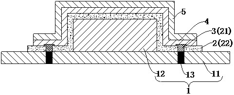
[0089] This embodiment proposes an electromagnetic shielding package and a manufacturing method thereof. The electromagnetic shielding package differs from Embodiment 1 only in that the conductive portion 3 of the electromagnetic shielding package is a continuous annular shape along the extending direction of the groove 21 . Conductive plastic. In the preparation method, a glue dispenser is used to dispense glue in the groove 21 to form the continuous ring-shaped conductive glue, and the conductive glue fills the groove 21. Image 6 shown. The rest are the same as those in Embodiment 1, and are not repeated here.

Embodiment 3

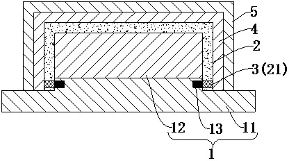
[0091] This embodiment proposes an electromagnetic shielding package and a preparation method thereof. The electromagnetic shielding package differs from Embodiment 2 only in that the minimum distance between the two electronic components 12 of the electromagnetic shielding package is 0.3 mm, and the shielding The thickness of the film 4 includes 50 μm or 100 μm. In the manufacturing method, the groove widths of the grooves 21 formed on the insulating film 2 include three types: 0.2 mm, 0.3 mm and 0.5 mm. The rest are the same as in Embodiment 2, and are not repeated here.


PUM

PropertyMeasurementUnit
Groove widthaaaaaaaaaa
Thicknessaaaaaaaaaa
Thicknessaaaaaaaaaa

Abstract

The invention relates to the technical field of integrated circuit board packaging, and discloses an electromagnetic shielding packaging body and a preparation method thereof.The electromagnetic shielding packaging body comprises an integrated circuit board, the integrated circuit board comprises a substrate and an electronic assembly, a grounding end is arranged on the outer peripheral face of the upper side of the substrate, the electronic assembly is arranged on the upper side face of the substrate, and the grounding end is arranged on the outer peripheral face of the substrate; the grounding end is positioned on the periphery of the electronic component; the insulating film is attached to the outer peripheral surface of the upper side of the electronic assembly and covers the grounding end, the electronic assembly is located between the insulating film and the substrate, a groove penetrating through the two side faces of the insulating film is formed in the insulating film, a conductive part is arranged in the groove, and one end of the conductive part is connected with the grounding end; and the shielding film is attached to the upper side surface of the insulating film and covers the groove, and the shielding film is connected with the other end of the conductive part.

Description

technical field [0001] The invention relates to the technical field of integrated circuit board packaging, in particular to an electromagnetic shielding package and a preparation method thereof. Background technique [0002] In an integrated circuit, in order to ensure the normal operation of the electronic components on the circuit board, it is generally necessary to do electromagnetic shielding for the electronic components, one is to comply with the electromagnetic compatibility (EMC) specification, and the other is to avoid the electronic components from being subjected to external electromagnetic interference (EMI) or to avoid Electromagnetic waves generated by electronic components radiate outward. The traditional method is to install the metal shield on the circuit board, and connect it with the ground terminal to build a "Faraday cage", which has an effective electromagnetic shielding effect. However, due to the large size of the metal shield, it is difficult for the...

Claims


Application Information

Patent Timeline
IPC IPC(8): H05K1/02H05K1/18H01L23/552
CPCH05K1/0216H05K1/181H01L23/552H05K2201/0707
Inventor 陈木久胡友根田锭坤许亚东刘学斌林志强陈巧刘晶云
Owner SHENZHEN JOHAN MATERIAL TECH CO LTD
Why Eureka
Try Eureka