Silicon carbide semiconductor device, power conversion device, and method for manufacturing silicon carbide semiconductor device
A silicon carbide and semiconductor technology, used in semiconductor devices, high-efficiency power electronic conversion, circuits, etc., can solve problems such as concentration and deterioration of semiconductor device withstand voltage, and achieve the effect of reducing JFET resistance and high withstand voltage.
- Summary
- Abstract
- Description
- Claims
- Application Information
AI Technical Summary
Problems solved by technology
Method used
Image
Examples
Embodiment approach 1
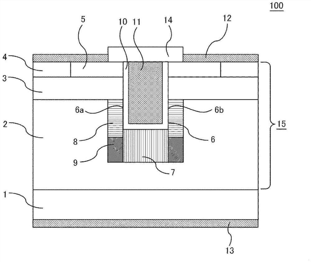
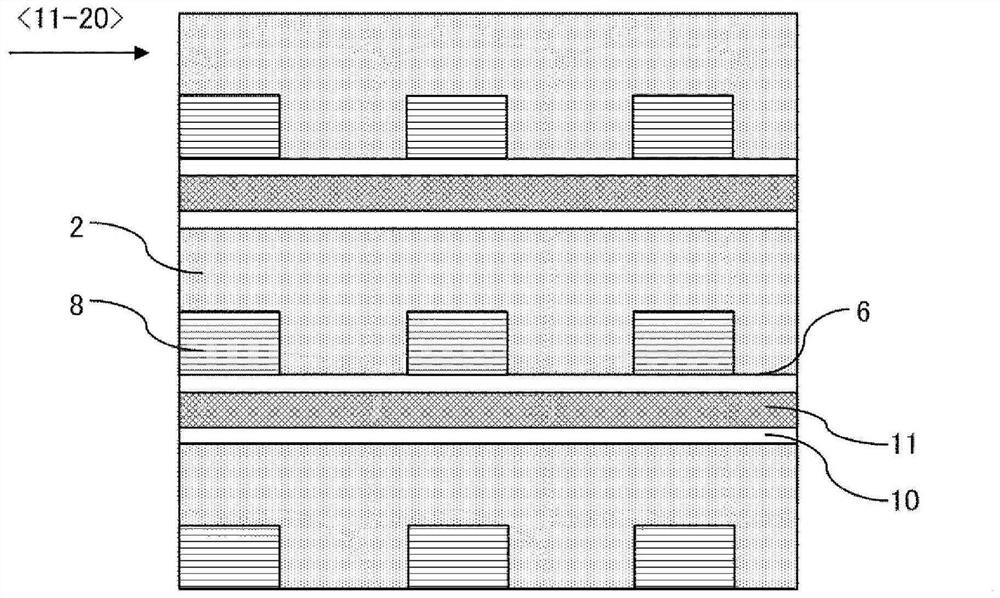
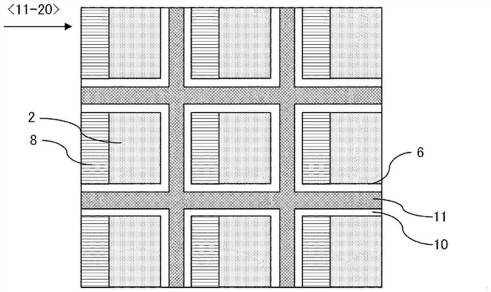
[0045] use Figure 1 to Figure 16 The silicon carbide semiconductor device of Embodiment 1 will be described.
[0046] First, use figure 1 The structure of the silicon carbide semiconductor device 100 will be described. figure 1 It is a cross-sectional view showing the silicon carbide semiconductor device 100 of the present embodiment.
[0047] Furthermore, in this disclosure, reference is made to figure 1 , the source electrode 12 side of the silicon carbide semiconductor device 100 with respect to the substrate 1 is defined as "upper", and the drain electrode 13 side with respect to the substrate 1 is defined as "lower".
[0048] like figure 1As shown, the silicon carbide semiconductor device 100 includes a substrate 1 , a gate electrode 11 , a source electrode 12 , a drain electrode 13 , an interlayer insulating film 14 , and a semiconductor layer 15 . The semiconductor layer 15 is provided on the upper side of the substrate 1 , and the drain electrode 13 is provided o...
Embodiment approach 2
[0128] use Figure 26 The silicon carbide semiconductor device of Embodiment 2 will be described. Figure 26 It is a cross-sectional view showing the silicon carbide semiconductor device 200 of the present embodiment.
[0129] The silicon carbide semiconductor device 200 is different from the silicon carbide semiconductor device 100 of the first embodiment in the structure of the protective layer 7 and the manufacturing method thereof. The other structures and manufacturing methods of the silicon carbide semiconductor device 200 are the same as those of the silicon carbide semiconductor device 100 , so the description is omitted.
[0130] like Figure 26 As shown, in the silicon carbide semiconductor device 200, the second-conductivity-type protective layer 7 provided below the trench 6 includes a first protective layer 7a with a high impurity concentration and a first protective layer 7a provided below the first protective layer 7a with an impurity concentration The second...
Embodiment approach 3
[0141] use Figure 27 The silicon carbide semiconductor device of the third embodiment will be described. Figure 27 It is a cross-sectional view showing the silicon carbide semiconductor device 300 of the present embodiment.
[0142] The silicon carbide semiconductor device 300 differs from the silicon carbide semiconductor device 100 of the first embodiment in the structures of the connection layer 8 and the electric field relaxation layer 9 and the manufacturing method thereof. The other structures and manufacturing methods of the silicon carbide semiconductor device 300 are the same as those of the silicon carbide semiconductor device 100 , so the description is omitted.
[0143] like Figure 27 As shown, in the silicon carbide semiconductor device 300 , the electric field relaxation layer 9 is provided so as to be in contact with the bottom surface of the connection layer 8 and the bottom surface of the protective layer 7 . That is, the electric field relaxation layer ...
PUM
 Abstract
Description
Claims
Application Information
 - R&D Engineer
- R&D Manager
- IP Professional
- Industry Leading Data Capabilities
- Powerful AI technology
- Patent DNA Extraction
Browse by: Latest US Patents, China's latest patents, Technical Efficacy Thesaurus, Application Domain, Technology Topic, Popular Technical Reports.
© 2024 PatSnap. All rights reserved.Legal|Privacy policy|Modern Slavery Act Transparency Statement|Sitemap|About US| Contact US: help@patsnap.com


