High-integration-level active dynamic loop filter
A high-integration, dynamic loop technology, applied in the field of filters, can solve the problems that affect the noise performance and even the function of the phase-locked loop, it is difficult to ensure a good matching of the charge pump current, and the noise performance is deteriorated, so as to increase the design flexibility, Effects of high power supply and substrate noise rejection, good jitter performance
- Summary
- Abstract
- Description
- Claims
- Application Information
AI Technical Summary
Problems solved by technology
Method used
Image

Examples
Embodiment 1
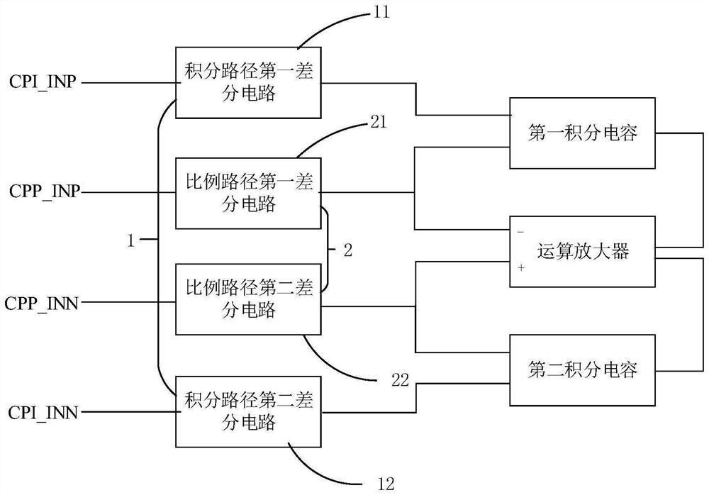
[0046] Please refer to image 3 and Figure 4 , image 3 is a structural block diagram of a highly integrated active dynamic loop filter provided by an embodiment of the present invention; Figure 4 It is a schematic structural diagram of a highly integrated active dynamic loop filter provided by an embodiment of the present invention. As shown in the figure, the highly integrated active dynamic loop filter of this embodiment includes: an integral path 1, a proportional path 2, and a first integral capacitor C INT1 , the second integrating capacitor C INT2 and operational amplifier OPA.
[0047] Among them, the integral path 1 and the proportional path 2 both adopt the differential structure, the integral path 1 with the internal symmetrical structure includes the first differential circuit 11 of the integral path and the second differential circuit 12 of the integral path, and the proportional path 2 with the internal symmetrical structure includes the proportional path ...
Embodiment 2
[0064] This embodiment specifically describes the working process of the highly integrated active dynamic loop filter of the first embodiment. Please refer to Figure 5 and Image 6 , Figure 5 It is a working schematic diagram of a highly integrated active dynamic loop filter provided by an embodiment of the present invention; Image 6 It is a working sequence diagram of a filter provided by an embodiment of the present invention.
[0065] The timing diagram of the first switch signal PH1 / second switch signal PH2, the first reset signal RES1 / second reset signal RES2 and the UP / DOWN is as follows Image 6 As shown, the UP / DOWN signal is the input signal of the previous stage charge pump, that is, the output of the PFD, which is used to control the first proportional current CPP_INP, the first integral current CPI_INP, the second proportional current CPP_INN and the second integral current CPI_INN Four input signals.
[0066] For the convenience of illustration, only look ...
PUM
 Abstract
Description
Claims
Application Information
 - R&D
- Intellectual Property
- Life Sciences
- Materials
- Tech Scout
- Unparalleled Data Quality
- Higher Quality Content
- 60% Fewer Hallucinations
Browse by: Latest US Patents, China's latest patents, Technical Efficacy Thesaurus, Application Domain, Technology Topic, Popular Technical Reports.
© 2025 PatSnap. All rights reserved.Legal|Privacy policy|Modern Slavery Act Transparency Statement|Sitemap|About US| Contact US: help@patsnap.com