Manufacturing method of semiconductor structure and manufacturing equipment of semiconductor structure

A manufacturing method and semiconductor technology, applied in the manufacture of semiconductor structures and semiconductor structure manufacturing equipment, can solve problems affecting the performance of semiconductor structures, residues are not easy to remove, etc., achieve good electrical properties, avoid direct contact, and reduce the degree of diffusion Effect

Pending Publication Date: 2022-07-19
CHANGXIN MEMORY TECH INC
View PDF3 Cites 0 Cited by
  • Summary
  • Abstract
  • Description
  • Claims
  • Application Information

AI Technical Summary

Problems solved by technology

However, in the existing removal process, the residues are not easy to be completely removed, and new residues are easily generated, thereby affecting the performance of the semiconductor structure

Method used


Image

  • Manufacturing method of semiconductor structure and manufacturing equipment of semiconductor structure
  • Manufacturing method of semiconductor structure and manufacturing equipment of semiconductor structure
  • Manufacturing method of semiconductor structure and manufacturing equipment of semiconductor structure

Examples


Embodiment Construction

[0026] It can be known from the background art that in the process of removing residues generated by etching, the residues are not easily removed completely, and new residues are easily generated, thereby affecting the quality of the semiconductor structure.

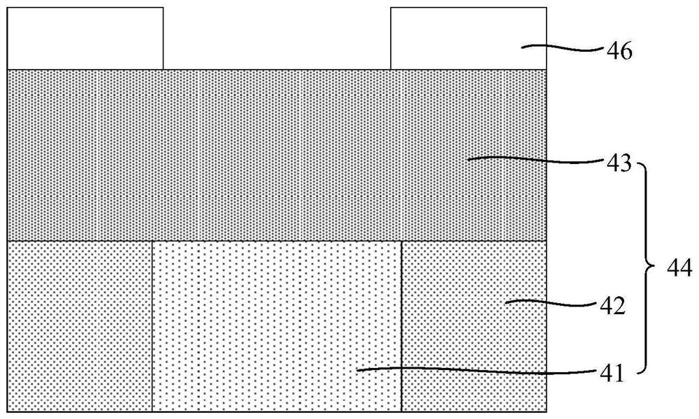
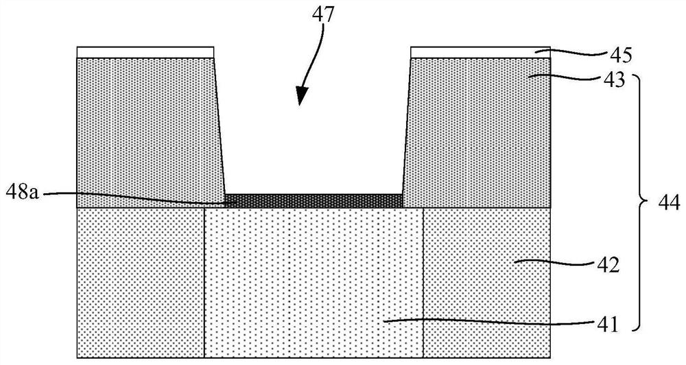
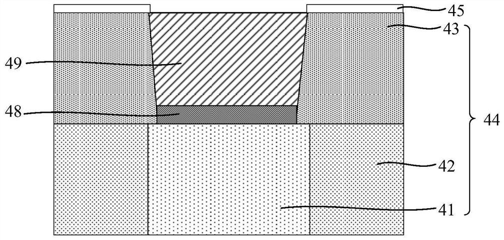
[0027] Figure 1-Figure 3 It is a schematic structural diagram of each step in a method for manufacturing a semiconductor structure. Specifically, refer to figure 1 , a substrate 44 is provided, the substrate 44 includes a first dielectric layer 42 , a first metal layer 41 located between adjacent first dielectric layers 42 , and a second dielectric layer located on the first metal layer 41 and the first dielectric layer 42 43 ; forming a patterned photoresist layer 46 on the second dielectric layer 43 . refer to figure 2 , with the patterned photoresist layer 46 (ref. figure 1 ) is a mask to etch the second dielectric layer 43 to form through holes 47 located in the second dielectric layer 43; during the etching p...


PUM

PropertyMeasurementUnit
heightaaaaaaaaaa

Abstract

The embodiment of the invention provides a semiconductor structure manufacturing method and semiconductor structure manufacturing equipment, and the semiconductor structure manufacturing method comprises the steps: providing a substrate; forming a patterned photoresist layer on the substrate, and etching the substrate by taking the patterned photoresist layer as a mask; after etching the substrate, carrying out plasma ashing treatment on the patterned photoresist layer and residues generated by etching by adopting a plasma ashing machine; the plasma ashing treatment process is carried out in an oxygen-free environment. According to the embodiment of the invention, the residues on the semiconductor structure can be removed without generating new residues, so that the electrical performance of the semiconductor structure can be improved.

Description

technical field [0001] Embodiments of the present invention relate to the field of semiconductors, and in particular, to a method for fabricating a semiconductor structure and a device for fabricating a semiconductor structure. Background technique [0002] Etching is a commonly used process technique in the fabrication of semiconductor structures. Etching is a major process of patterning associated with photolithography. Photolithography etching refers to first exposing the photoresist by photolithography, and then etching the part to be removed by other means. [0003] After etching, residues such as photoresist and oxide layers are typically removed using a combination of dry and wet processes. For example, oxygen plasma ashing is used first, followed by wet chemical cleaning with organic solvents at high temperature. However, in the existing removal process, the residues are not easily removed completely, and new residues are easily generated, thereby affecting the pe...

Claims


Application Information

Patent Timeline
Patent Type & Authority Applications(China)
IPC IPC(8): H01L21/768H01L21/67
CPCH01L21/76814H01L21/67069H01L2221/101H01L21/768H01L21/67H01L21/687H01L21/027H01L21/683
Inventor 李世鸿
Owner CHANGXIN MEMORY TECH INC
Why Eureka
Try Eureka