Semiconductor structure and forming method thereof

A technology of semiconductor and isolation structure, applied in the field of semiconductor structure and its formation, can solve the problems of unfavorable device performance, metal gate material not easy to fill, unstable gate structure performance, etc., to achieve the effect of improving performance

Pending Publication Date: 2022-07-29
SEMICON MFG INT (SHANGHAI) CORP +1
View PDF0 Cites 0 Cited by
  • Summary
  • Abstract
  • Description
  • Claims
  • Application Information

AI Technical Summary

Problems solved by technology

In HKMG technology, in the process of replacing the polysilicon gate with a metal gate, limited by the three-dimensional structure and small size of the FinFET device, the metal gate material is not easy to fill, resulting in unstable performance of the formed gate structure, which is not conducive to the improvement of device performance.
[0004] In conclusion, the technology of existing FinFET devices needs to be further improved

Method used


Image

  • Semiconductor structure and forming method thereof
  • Semiconductor structure and forming method thereof
  • Semiconductor structure and forming method thereof

Examples


Embodiment Construction

[0028] It should be noted that "surface" and "upper" in this specification are used to describe the relative positional relationship in space, and are not limited to whether they are in direct contact.

[0029]As described in the background art, the performance of the semiconductor structure formed by the existing FinFET technology needs to be improved. Now combined with a semiconductor structure to illustrate the analysis.

[0030] Figure 1 to Figure 5 It is a schematic diagram of the formation process of a semiconductor structure.

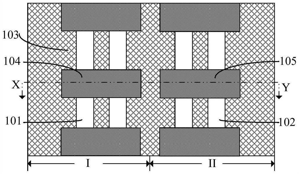
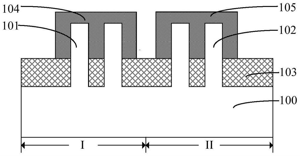
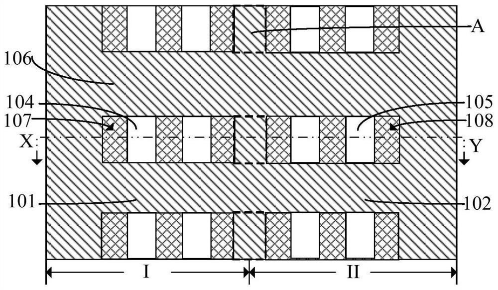
[0031] Please refer to figure 1 and figure 2 , figure 1 is a top view, figure 2 is along the figure 1 A schematic diagram of a cross-sectional structure in the XY direction in the middle, a substrate is provided, the substrate includes a base 100, and the base 100 includes a first area I and a second area II adjacent to the first area I, located in the first area Several first fins 101 on I, several second fins 102 on the second regio...


PUM


Abstract

The invention discloses a semiconductor structure and a forming method thereof, and the method comprises the steps: enabling an opening to expose a part of a first fin part, a part of a second fin part and a part of a third region, enabling a second direction to be perpendicular to a first direction, and enabling the third region in the opening to be provided with a first isolation structure, the first isolation structure comprises a first isolation layer and a second isolation layer located on the first isolation layer, and the size of the first isolation layer in the second direction is larger than that of the second isolation layer in the second direction; forming a first gate on the first region in the opening; a second gate is formed on the second region within the opening. The size of the top of the opening is larger than the size of the bottom of the opening in the second direction, filling of a grid material in the opening is facilitated, the situation that the top of the opening is closed earlier than the bottom of the opening is avoided, and the performance of the formed first grid and the second grid is improved.

Description

technical field [0001] The present invention relates to the technical field of semiconductor manufacturing, and in particular, to a semiconductor structure and a method for forming the same. Background technique [0002] In the existing semiconductor field, the fin field effect transistor (FinFET) is an emerging multi-gate device. Compared with the planar metal-oxide semiconductor field effect transistor (MOSFET), the fin field effect transistor has more It has strong short-channel suppression ability and stronger working current, and has been widely used in various semiconductor devices. [0003] At present, the semiconductor industry uses a metal gate to replace the polysilicon gate electrode to solve the problems such as threshold voltage Vt drift, polysilicon gate depletion effect, excessive gate resistance and Fermi level pinning. The technology of replacing SiON with high-K dielectric material and replacing polysilicon gate with metal gate is called HKMG process techn...

Claims


Application Information

Patent Timeline
Patent Type & Authority Applications(China)
IPC IPC(8): H01L29/78H01L29/423H01L21/336
CPCH01L29/66795H01L29/785H01L29/42356
Inventor 周飞
Owner SEMICON MFG INT (SHANGHAI) CORP
Why Eureka
Try Eureka