Preparation method of P-type nitride epitaxial structure, epitaxial structure and semiconductor device

An epitaxial structure, nitride technology, applied in semiconductor devices, semiconductor/solid-state device manufacturing, electrical components, etc., can solve problems such as the generation of Mg cones and fog flakes, poor surface quality and crystal quality of p-type GaN epitaxy, to improve Effects of crystal quality, increased carrier concentration, and reduced surface formation energy

Pending Publication Date:
View PDF0 Cites 0 Cited by
  • Summary
  • Abstract
  • Description
  • Claims
  • Application Information

AI Technical Summary

Problems solved by technology

[0002] Growing high-quality P-type GaN has always been a difficult problem in the field of semiconductor technology, especially when the carrier concentration is greater than 1E18cm -3 When the traditional method increases the carrier concentration of p-type GaN by increasing the Mg concentration, the corresponding p-type GaN epitaxial surface quality and crystal quality become very poor, resulting in Mg cones and haze

Method used


Image

  • Preparation method of P-type nitride epitaxial structure, epitaxial structure and semiconductor device
  • Preparation method of P-type nitride epitaxial structure, epitaxial structure and semiconductor device
  • Preparation method of P-type nitride epitaxial structure, epitaxial structure and semiconductor device

Examples


preparation example Construction

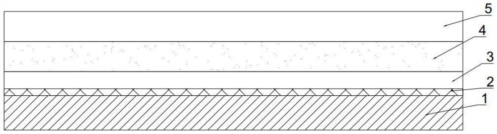
[0034] Specifically, refer to figure 1 , the present invention provides a preparation method of a P-type nitride epitaxial structure, comprising the following steps:

[0035] Provide substrate 1;

[0036] On the substrate 1, grow a U-type nitride layer, a lightly-doped P-type nitride layer 4 and a highly-doped P-type nitride layer 5 grown by using a delta doping method in sequence;

[0037] in the cavity N 2 Annealing in atmosphere;

[0038] The highly doped P-type nitride layer 5 grows periodically, and each period of growth includes the following steps:

[0039] Feed N source and Group III metal source, and add surfactant to form a non-doped nitride layer, and the surfactant is In;

[0040] Cut off the three-group metal source and surfactant, and carry out N source purging to desorb the three-group metal atoms;

[0041] The doping source is passed through, the doping elements of the doping source include Mg and Cu, the Mg element is the main doping element, and the Cu e...

Embodiment 1

[0054] This embodiment prepares and tests the P-type GaN structure, which specifically includes the following steps:

[0055] (1) Take sapphire as the substrate;

[0056] (2) After growing the undoped GaN buffer layer of about 50 nm, grow the undoped GaN layer of about 2 μm as the bottom layer;

[0057] (3) Grow a low-doped p-type GaN layer of about 2 μm, the growth pressure is 150 Torr, and the growth temperature is 1090 °C;

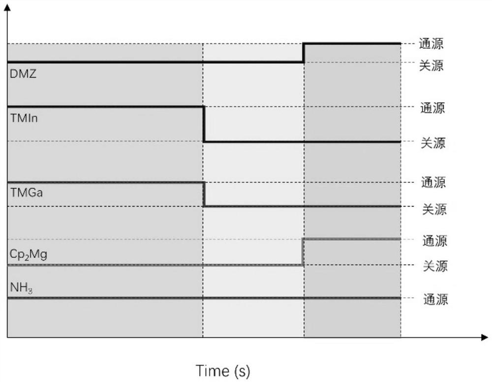
[0058] (4) Use the delta doping method to grow a high-doped p-type GaN layer of about 550 nm, the growth pressure is 500 Torr, the growth temperature is 1045, and the growth is one cycle according to the following steps, and a total of 300 cycles of cyclic growth:

[0059] (41) Keep NH 3 Pass in, and pass in the TMGa and TMIn sources for 15 seconds, the flow rate of TMGa is 40sccm, and TMIn:TMGa=10%;

[0060] (42) then turn off the TMGa source and the TMIn source, and only pass NH purging for 4 seconds, so that the three-group metal atoms are desorbe...

Embodiment 2

[0079] In order to further illustrate the effect of high voltage on the heavily doped P-type GaN layer, this embodiment changes the growth pressure of the heavily doped P-type GaN layer compared with Embodiment 1, and the rest is the same as that of Embodiment 1;

[0080] 1) the growth pressure of step 4) in Example 1 is 400 Torr;

[0081] 2) the growth pressure of step 4) in Example 1 is 600 Torr;

[0082] The P-type GaN structure samples prepared under the two growth pressures in the above-mentioned Example 1 and Example 2 were subjected to the Hall effect test and the XRD test respectively under the test conditions of the Hall current of 0.0049mA, and the obtained P-type GaN structure samples The layer results are shown in Table 2:

[0083] Table 2:

[0084]

[0085] The results show that: as the growth pressure increases, the carrier concentration increases (500 Torr in Example 1 is higher than that in Example 2 (1)), that is, the doping rate of Mg increases, and high...


PUM

PropertyMeasurementUnit
thicknessaaaaaaaaaa
thicknessaaaaaaaaaa

Abstract

The invention discloses a preparation method of a P-type nitride epitaxial structure, the epitaxial structure and a semiconductor device. The method comprises the following steps: providing a substrate; sequentially growing a U-type nitride layer, a lightly doped P-type nitride layer and a highly doped P-type nitride layer which is grown by adopting a delta doping method on the substrate; annealing is carried out in the cavity; wherein the highly-doped P-type nitride layer grows periodically, and the growth of each period comprises the following steps of: introducing an N source and a III-group metal source, and adding a surface active agent to form a non-doped nitride layer; cutting off the III-group metal source and the surfactant, and carrying out N-source purging; a doping source is introduced, doping elements of the doping source comprise Mg and Cu, the Mg element is a main doping element, and the Cu element is an auxiliary doping element. According to the method, the carrier concentration of the P-type nitride is improved, and meanwhile good crystal quality and epitaxial surface quality are achieved.

Description

technical field [0001] The present invention relates to the technical field of semiconductors, in particular to a preparation method of a P-type nitride epitaxial structure, an epitaxial structure and a semiconductor device. Background technique [0002] Growing high-quality P-type GaN has always been a difficult problem in the field of semiconductor technology, especially the growth carrier concentration is greater than 1E18cm -3 When the traditional method increases the carrier concentration of p-type GaN by increasing the Mg concentration, the corresponding p-type GaN epitaxial surface quality and crystal quality become very poor, resulting in Mg cones and fog flakes. SUMMARY OF THE INVENTION [0003] The purpose of the present invention is to provide a preparation method of a P-type nitride epitaxial structure, an epitaxial structure and a semiconductor device, which can improve the carrier concentration and have better crystal quality and epitaxial surface quality. ...

Claims


Application Information

Patent Timeline
Patent Type & Authority Applications(China)
IPC IPC(8): H01L21/205H01L29/20H01L29/207
CPCH01L21/02458H01L21/02499H01L21/0254H01L21/02579H01L21/0262H01L21/02694H01L29/2003H01L29/207Y02P70/50
Inventor 周溯沅闫其昂王国斌
Why Eureka
Try Eureka