Embedded flash memory and preparation method thereof

An embedded and flash memory technology, which is applied in the direction of semiconductor devices, electrical components, circuits, etc., can solve the problems of increased leakage current of small-sized embedded flash memory, and achieve the effect of reducing leakage current, satisfying the gradual reduction of area, and reducing the thickness

Pending Publication Date: 2022-08-05
SHANGHAI HUAHONG GRACE SEMICON MFG CORP +1
View PDF0 Cites 0 Cited by
  • Summary
  • Abstract
  • Description
  • Claims
  • Application Information

AI Technical Summary

Problems solved by technology

However, as the area of ​​embedded flash memory gradually shrinks, the thickness of the sidewall of the corresponding flash memory unit and the sidewall of the logic unit also gradually decrease, and the reduction of the thickness of the sidewall leads to a sharp increase in the leakage current of the small-sized embedded flash memory

Method used


Image

  • Embedded flash memory and preparation method thereof
  • Embedded flash memory and preparation method thereof
  • Embedded flash memory and preparation method thereof

Examples


preparation example Construction

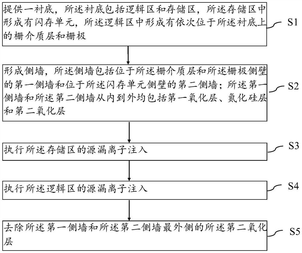
[0047] Embodiments of the present invention provide a method for preparing an embedded flash memory, such as figure 1 shown, including:

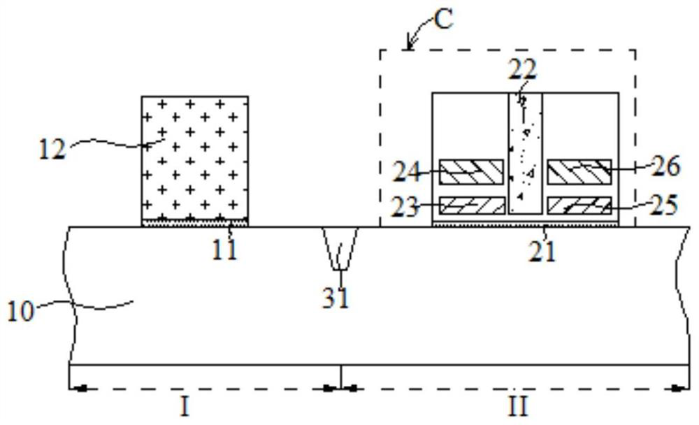
[0048] Step S1, providing a substrate, the substrate includes a logic area and a storage area, flash memory cells are formed in the storage area, and a gate dielectric layer and a gate electrode sequentially located on the substrate are formed in the logic area ;

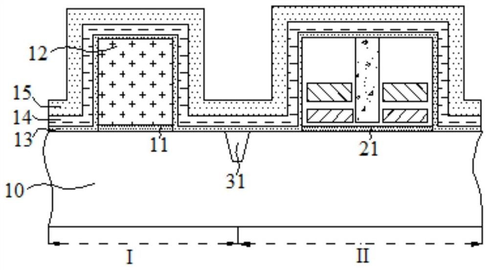
[0049] Step S2, forming spacers, including a first spacer located on the sidewall of the gate dielectric layer and the gate, and a second spacer located on the sidewall of the flash memory cell; the first spacer and the second spacer includes a first oxide layer, a silicon nitride layer and a second oxide layer from inside to outside;

[0050] Step S3, performing source-drain ion implantation of the storage area;

[0051] Step S4, performing source-drain ion implantation of the logic region;

[0052]Step S5, removing the second oxide layer on the outermost side of the first sp...


PUM

PropertyMeasurementUnit
thicknessaaaaaaaaaa
thicknessaaaaaaaaaa
thicknessaaaaaaaaaa

Abstract

The invention provides an embedded flash memory and a preparation method thereof, after a side wall material layer is etched to form a side wall, a second oxide layer on the outermost side of the side wall is removed without etching, and after source and drain ions are injected to form a source electrode and a drain electrode, the second oxide layer in the side wall is removed. On one hand, ions are prevented from entering the substrate part under the side wall to influence the performance of the flash memory in the source-drain ion implantation process of the logic region and the storage region; and on the other hand, during source-drain ion implantation, the thickness of the side wall is the sum of the thicknesses of the first oxide layer, the silicon nitride layer and the second oxide layer, and the thickness of the side wall is relatively large, so that the formed source electrode and drain electrode are farther away from the channel, and the leakage current of the embedded flash memory is effectively reduced. According to the invention, after ion implantation is completed, the second oxide layer on the outermost side of the first side wall and the second side wall is removed, so that the thickness (size) of each side wall of the logic region and the storage region is reduced; the leakage current of the embedded flash memory is reduced, and meanwhile, the requirement that the area of the embedded flash memory is gradually reduced is met.

Description

technical field [0001] The invention belongs to the technical field of integrated circuit manufacturing, and in particular relates to an embedded flash memory and a preparation method thereof. Background technique [0002] Memory is used to store a large amount of digital information. Over the years, the advancement of process technology and market demand have spawned more and more high-density various types of memory, such as RAM (random access memory), DRAM (dynamic random access memory), etc. Among them, flash memory That is, FLASH has become the mainstream of non-volatile semiconductor storage technology. Among various FLASH devices, embedded flash memory is a type of system-on-chip (SOC), which integrates logic circuit modules and flash memory circuit modules in an integrated circuit. , widely used in smart cards, microcontrollers and other products. [0003] The embedded flash memory includes flash memory cells in the storage area and logic cells in the logic area, an...

Claims


Application Information

Patent Timeline
Patent Type & Authority Applications(China)
IPC IPC(8): H01L27/11521H01L27/11526H01L21/28H10B41/30H10B41/40
CPCH01L29/40114H10B41/30H10B41/40
Inventor 周海洋王会一
Owner SHANGHAI HUAHONG GRACE SEMICON MFG CORP
Why Eureka
Try Eureka