
Electronic structure and manufacturing method thereof

A technology of electronic structure and production method, which is applied in the fields of printed circuit manufacturing, cable/conductor manufacturing, circuit, etc., can solve the problem that low-temperature conductive silver paste cannot meet high adhesion and solderability at the same time, so as to meet the requirements of solderability and ensure the combination The effect of intensity

Pending Publication Date: 2022-08-05
BEIJING DREAM INK TECH CO LTD
View PDF5 Cites 0 Cited by
  • Summary
  • Abstract
  • Description
  • Claims
  • Application Information

AI Technical Summary

Problems solved by technology

[0006] In view of this, an object of the present invention is to propose a method for making an electronic structure, so as to solve the problem that the low-temperature conductive silver paste in the prior art cannot simultaneously meet the needs of users with high adhesion and solderability

Method used


Image

  • Electronic structure and manufacturing method thereof
  • Electronic structure and manufacturing method thereof
  • Electronic structure and manufacturing method thereof

Examples


Embodiment Construction

[0024] Reference will now be made in detail to various embodiments of the present disclosure, examples of which are illustrated in the accompanying drawings. When described in conjunction with these embodiments, it should be understood that the embodiments are not intended to limit the disclosure to these embodiments. On the contrary, the present disclosure is intended to cover alternatives, modifications and equivalents, which may be included within the spirit and scope of the present disclosure as defined by the appended claims. Furthermore, in the following detailed description of the present disclosure, numerous specific details are set forth in order to provide a thorough understanding of the present disclosure. It should be understood, however, that the present disclosure may be practiced without these specific details. In other instances, well-known methods, procedures, components and circuits have not been described in detail so as not to unnecessarily obscure aspects...


PUM

PropertyMeasurementUnit
sizeaaaaaaaaaa
quality scoreaaaaaaaaaa

Abstract

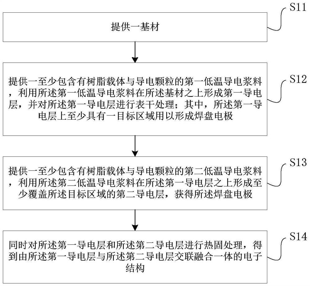
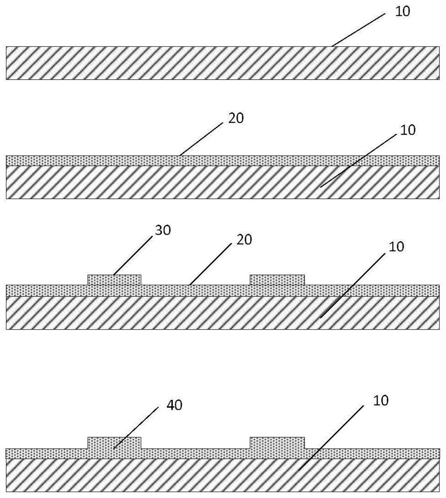
The invention discloses an electronic structure and a manufacturing method thereof, and relates to the technical field of electronic manufacturing. The manufacturing method of the electronic structure comprises the following steps: providing a base material; forming a first conductive layer on the base material by using the first low-temperature conductive slurry, and performing surface drying treatment on the first conductive layer; forming a second conductive layer at least covering the target area on the first conductive layer by using second low-temperature conductive slurry to obtain a bonding pad electrode; and performing thermosetting treatment on the first conductive layer and the second conductive layer at the same time to obtain an electronic structure in which the first conductive layer and the second conductive layer are crosslinked and fused into a whole. The first conductive layer in direct contact with the base material is formed by using the first low-temperature conductive slurry with low-conductive particles and high resin, and the pad electrode is formed on the first conductive layer by using the second low-temperature conductive slurry with high-conductive particles and low resin; in addition, the first conducting layer and the second conducting layer are thermally cured at the same time, and the high-adhesion and weldable effects of the electronic structure are achieved.

Description

technical field [0001] The invention belongs to the technical field of electronic manufacturing, and in particular relates to an electronic structure and a manufacturing method thereof. Background technique [0002] As an emerging electronic circuit additive manufacturing raw material, conductive paste is often used to form the electronic structure required by users by printing and other methods. Compared with traditional copper foil and aluminum foil etching technologies, the printing conductive paste process has low cost, no Contaminated, fast, high-volume manufacturing advantages. [0003] Differentiated by sintering and curing temperature, conductive pastes are generally divided into high-temperature conductive pastes and low-temperature conductive pastes. In high-temperature conductive pastes, glass powder is mainly used as a binder for conductive particles, and the sintering temperature generally needs to reach thousands of degrees. , Even if the expensive low-melting...

Claims


Application Information

Patent Timeline
Patent Type & Authority Applications(China)
IPC IPC(8): H05K3/00H05K3/40H05K1/09H05K1/11H01B13/00H01B1/22H01B5/14
CPCH05K3/00H05K3/40H05K3/4007H05K1/092H05K1/11H01B13/0026H01B1/22H01B5/14
Inventor 吕文峰鲁强王莉
Owner BEIJING DREAM INK TECH CO LTD
Learn More