Reversible molecular electronic device based on technique of scan tunnel microscope and its manufacturing method

An electronic device and scanning tunneling technology, applied in the field of molecular electronic devices

Inactive Publication Date: 2005-06-15
FUDAN UNIV
View PDF0 Cites 0 Cited by
  • Summary
  • Abstract
  • Description
  • Claims
  • Application Information

AI Technical Summary

Problems solved by technology

[0003] The function of molecular electronic devices is mainly based on the behavior and properties of individual molecules. Many current microelectronic technologies can no longer meet the requirements, so a new process technology is required

Method used


Image

  • Reversible molecular electronic device based on technique of scan tunnel microscope and its manufacturing method
  • Reversible molecular electronic device based on technique of scan tunnel microscope and its manufacturing method
  • Reversible molecular electronic device based on technique of scan tunnel microscope and its manufacturing method

Examples


Embodiment 1

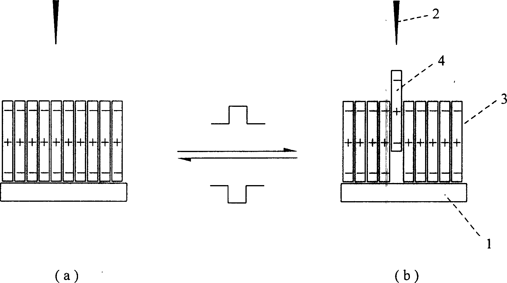
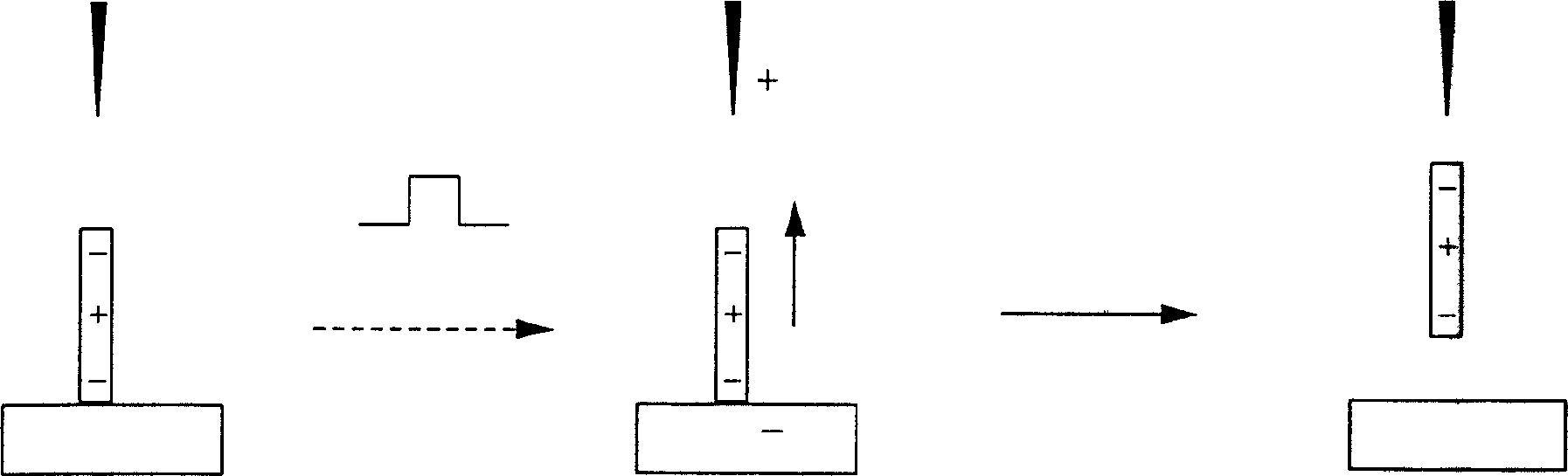
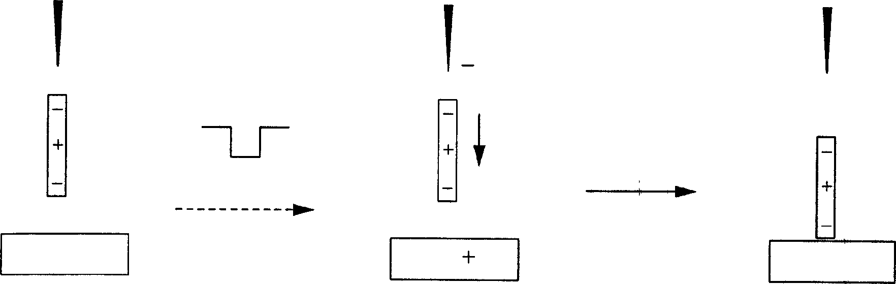
[0094] Embodiment 1 Prepare Ag single crystal thin film by epitaxial method on the newly stripped mica surface, then prepare vertically oriented CPVB monolayer film on the surface of Ag single crystal thin film (solvent adopts acetonitrile-benzene mixed solution, CPVB solution Concentration is 10 -5 About M, immerse the base in the base to absorb into a film). The Ag substrate is used as the substrate of STM, and the STM probe adopts Pt-Ir alloy wire. The STM instrument works in the constant high mode, and the working voltage is 0.005-0.1 volts, and the thin film device is in the "0" state at this time. A positive square wave pulse voltage (1-4 volts, the probe is positive and the substrate is negative) is applied between the STM probe and the substrate, and the CPVB molecules under the needle tip are pulled up for a certain distance, that is, the "1" state, This process is "writing". At the same position, if a reverse pulse voltage (1-4 volts, the base is positive), the CP...

Embodiment 2

[0096] Example 2 The compound uses PDVB, the solvent uses acetone, and the solution concentration is 10 -6 -10 -5 M. The preparation process of the film layer and the device assembly are the same as Example 1. The external working voltage of its reversible conversion is a square wave pulse voltage of 3-4 volts, that is, writing and erasing can be realized, and can be repeated.

Embodiment 3

[0097] Example 3 The compound uses ACVB, the solvent uses acetone-acetonitrile mixed solution, and the solution concentration is 5×10 -5 M or so. The preparation process of the film layer and device assembly are the same as Example 1. The external working voltage of its reversible conversion is a square wave pulse voltage of 3-4 volts, that is, writing and erasing can be realized, and can be repeated.


PUM


Abstract

The invention belongs to the technical field of molecular electronic devices, and in particular relates to an electrically reversible molecular electronic device based on scanning tunneling microscopy technology and a manufacturing method thereof. This molecular electronic device consists of a substrate, an organic molecular layer, and a probe. Among them, the substrate adopts an atomically flat conductive surface, the probe adopts a needle tip in a scanning tunneling microscope, and the organic molecular layer is a vertically oriented monolayer. The organic molecules are elongated π-conjugated molecules containing polar groups. This molecular electronic device can be reversibly switched with an external forward and reverse pulse voltage, that is, it can be erased and written, and can be read with a very low operating voltage. The molecular electronic device of the invention can be used as an electrically erasable ultra-high-density memory, a molecular switch, a logic element, etc., and has wide application value in molecular computers.

Description

technical field [0001] The invention belongs to the technical field of molecular electronic devices, and in particular relates to an electrically reversible molecular electronic device based on scanning tunneling microscopy technology and its production, use and application. technical background [0002] The development trend of large-scale integrated circuits is that the size is constantly shrinking, and it is about to enter the era of nanoelectronic devices. There are two ways to develop nanoelectronic devices: one is to use the original microelectronic processing technology to keep the size of the device down to the nanoscale; the other is to realize the function of electronic devices by manipulating and assembling organic molecules, that is, molecular electronic devices . The latter is a new field, and a lot of manpower and material resources have been invested in research and development at home and abroad. [0003] The functions of molecular electronic devices are ma...

Claims


Application Information

Patent Timeline
Patent Type & Authority Patents(China)
IPC IPC(8): G01Q60/16H01L51/00
CPCB82Y10/00H10K10/701
Inventor 徐伟华中一
Owner FUDAN UNIV
Why Eureka
Try Eureka