
Method for preparing self-aligning silicide of metal oxide semiconductor

A self-aligned silicide and oxide technology, used in semiconductor/solid-state device manufacturing, semiconductor devices, electrical components, etc., can solve the complex preparation method, the unavoidable cobalt titanium cobalt silicide peak, junction leakage current and other problems. Problems such as breakdown voltage drop

Inactive Publication Date: 2005-06-15
WINBOND ELECTRONICS CORP
View PDF4 Cites 0 Cited by
  • Summary
  • Abstract
  • Description
  • Claims
  • Application Information

AI Technical Summary

Problems solved by technology

Third, because cobalt-silicon is closer to the mid-bandgap level than titanium-silicon, cobalt metal or cobalt silicide will penetrate into the interior of the silicon substrate during the silicidation reaction to generate a spike. Phenomenon, in the shallow junction (shallow junction) structure is easy to cause junction leakage current and breakdown voltage drop, therefore, the preparation method of cobalt silicide is also more complicated than the preparation method of titanium silicide
However, the above methods still cannot avoid the formation of cobalt titanide and cobalt silicide spike phenomenon

Method used


Image

  • Method for preparing self-aligning silicide of metal oxide semiconductor
  • Method for preparing self-aligning silicide of metal oxide semiconductor
  • Method for preparing self-aligning silicide of metal oxide semiconductor

Examples


Embodiment Construction

[0052] 2(a) to 2(e) are flow charts according to the first preferred embodiment of the present invention. First, a silicon substrate 201 is provided, the surface of the silicon substrate 201 has a gate 203, the lightly doped region 206 is located in the silicon substrate below the two sides of the gate 203, and the spacer 204 is located on the side of the gate 203 wall, and field oxide layer 202, as shown in Figure 2(a). Next, a heavy doping step is performed using the spacer 204 and the gate 203 as a mask, so that only the region below the spacer 204 remains in the lightly doped region 206, and the rest of the region forms the source / The drain region 205 is called a lightly doped drain (LDD) design, as shown in FIG. 2( b ).

[0053] After that, a cobalt metal layer 207 is deposited on the surface of the field oxide layer 202, the source / drain region 205, the spacer 204 and the gate 203 by chemical deposition (CVD) or physical vapor deposition (PVD), such as Figure 2(c) sho...


PUM


Abstract

The invention provides a method for preparing a self-aligned silicide of a metal-oxide-semiconductor (MOS) transistor. In the invention, an ion implantation step is performed before the metal-oxide-semiconductor transistor is subjected to self-aligned silicide treatment, and the implanted Ions (such as: fluorine, chlorine, bromine, iodine, boron and boron difluoride) will first react with the silicon substrate and the surface of the gate, and produce a barrier effect (barrier efreet) in the silicidation process, which can prevent cobalt metal or It is cobalt silicide that infiltrates into the gate or source / drain region to produce a spike phenomenon, which avoids causing junction leakage or reducing the breakdown voltage of the metal oxide semiconductor transistor.

Description

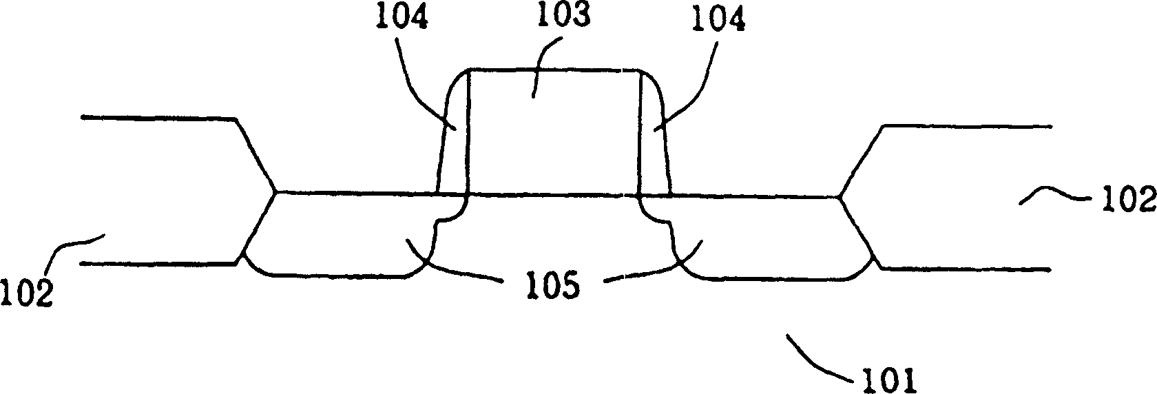
technical field [0001] The invention relates to a method for preparing a self-aligned silicide of a metal-oxide-semiconductor transistor, in particular to a cobalt silicide (CoSi 2 ) preparation method. Background technique [0002] With the increase of semiconductor element integration (integrity), in order to avoid the leakage junction (Leaky Junction) between the gate and the source / drain, a self-aligned silicide (self-aligned silicification, also known as salicification) is In the semiconductor process, a silicide layer is formed on the surface of the source / drain region and the gate region by silicide treatment to avoid leakage current. [0003] The most common material commonly used to prepare the silicide layer is titanium (Ti) metal, and its preparation process is as follows Figures 1(a) to 1(d) shown. First, a silicon substrate 101 with metal oxide semiconductor transistors is provided, as shown in FIG. 1( a ). The metal-oxide-semiconductor transistor includes a...

Claims


Application Information

Patent Timeline
IPC IPC(8): H01L21/336H01L29/78
Inventor 陈伟梵廖文翔张明伦
Owner WINBOND ELECTRONICS CORP
Learn More