Electrical device having PTC conductive polymer
An electronic component, conductive polymer technology, applied in the field of electronic components with PTC conductive polymer, can solve problems such as uneven thickness
- Summary
- Abstract
- Description
- Claims
- Application Information
AI Technical Summary
Problems solved by technology
Method used
Image
Examples
Embodiment 1
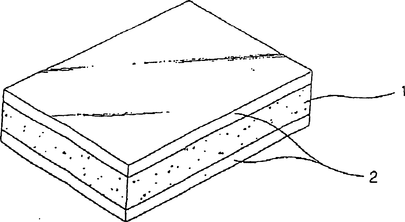
[0028] The PTC conductive polymer is prepared by mixing polyethylene and carbon black. The surface roughness of an electroplated copper foil is controlled between 5 and 10 μm by electrolytic plating. Then, an electroless nickel metal-plating process with a thickness of 1 μm was formed on the electroplated copper foil through a degreasing process, a pickling process, a driving process, a photosensitive treatment process, an electroless nickel metal-plating process, and a rinsing process. layers to make electrodes. The electrodes are welded on both sides of the PTC conductive polymer similar to a sandwich, resulting in image 3 electronics shown.
Embodiment 2
[0030] The PTC conductive polymer is prepared by mixing polyethylene and carbon black. The surface roughness of an electroplated copper foil is controlled between 5 and 10 μm by electrolytic plating. Then, an electroless nickel metal-plating process with a thickness of 10 μm was formed on the electroplated copper foil through a degreasing process, a pickling process, a driving process, a photosensitive treatment process, an electroless nickel metal-plating process, and a rinsing process. layers to make electrodes. The electrodes are welded on both sides of the PTC conductive polymer similar to a sandwich, resulting in image 3 electronics shown.
Embodiment 3
[0032] An electronic device was produced in the same manner as in Example 1. However, the drive and photosensitive treatment processes are removed during the electroless-plating process, and the electroless nickel metal-plating process is carried out following the pickling process. Chromium metal is then overlaid on the electroless nickel metal-plated layer by displacement plating in a chromium bath.
PUM
| Property | Measurement | Unit |
|---|---|---|
| surface roughness | aaaaa | aaaaa |
| thickness | aaaaa | aaaaa |
| thickness | aaaaa | aaaaa |
Abstract
Description
Claims
Application Information


