Method for producing plate shape body and semiconductor device

A manufacturing method and technology of plate-like bodies, which are applied in semiconductor/solid-state device manufacturing, semiconductor devices, semiconductor/solid-state device components and other directions, can solve problems such as warpage, strength reduction, complex process, etc., and achieve low sheet resistance, The effect of dense surface flatness and high connection accuracy

Inactive Publication Date: 2006-01-18
SANYO ELECTRIC CO LTD
View PDF0 Cites 0 Cited by
  • Summary
  • Abstract
  • Description
  • Claims
  • Application Information

AI Technical Summary

Problems solved by technology

However, if the thickness of the standard frame 20 itself becomes thinner, its strength will decrease, warping will occur on the standard frame 20, and the lead end 26 will be deformed and displaced.
In particular, since the connection pad 23 connected to the thin metal wire 24 is not supported, there are problems such as deformation and warpage.
[0020] Moreover, the part shown by the arrow in Figure 18 is where the lead terminal 26 is drawn out from the side of the package. The gap between the lead terminal 26 and the lead terminal 26 cannot be butted with the upper metal mold 32 and the lower metal mold, and the occurrence of burrs cannot be avoided.
[0021] As shown above, the standard frame is limited in microfabrication, and the total size of the package cannot be made smaller. However, if the process is considered, there must be a method to prevent the standard frame from warping, and at the same time, there must be a process for eliminating burrs. The suspension wire 7 and the tie bar 8 are cut, so in addition to the complicated process, the lead wire deformation or punching problem in the tie bar cutting process becomes the cause of the low reliability of the semiconductor device.

Method used


Image

  • Method for producing plate shape body and semiconductor device
  • Method for producing plate shape body and semiconductor device
  • Method for producing plate shape body and semiconductor device

Examples


Embodiment Construction

[0098] Description of the first embodiment of the plate-shaped body

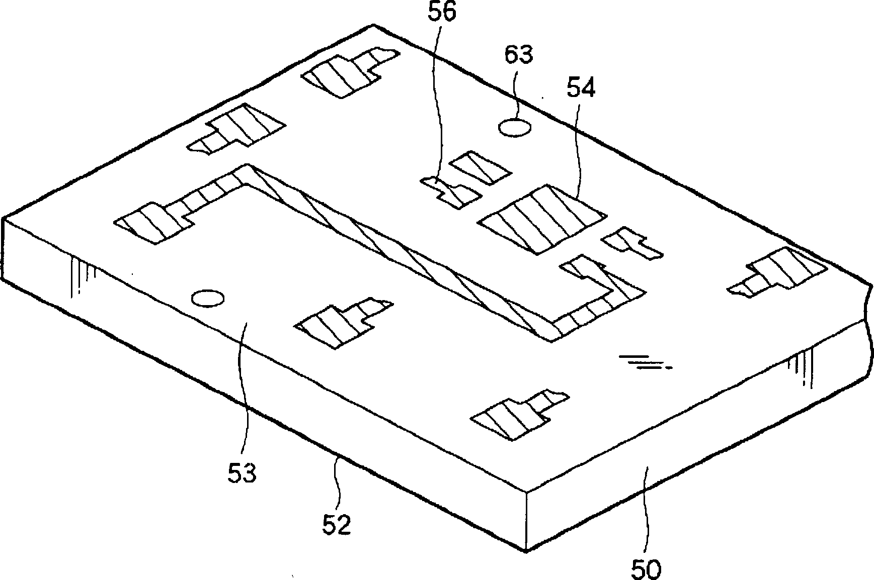
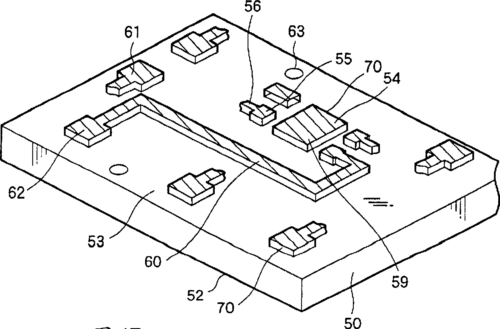
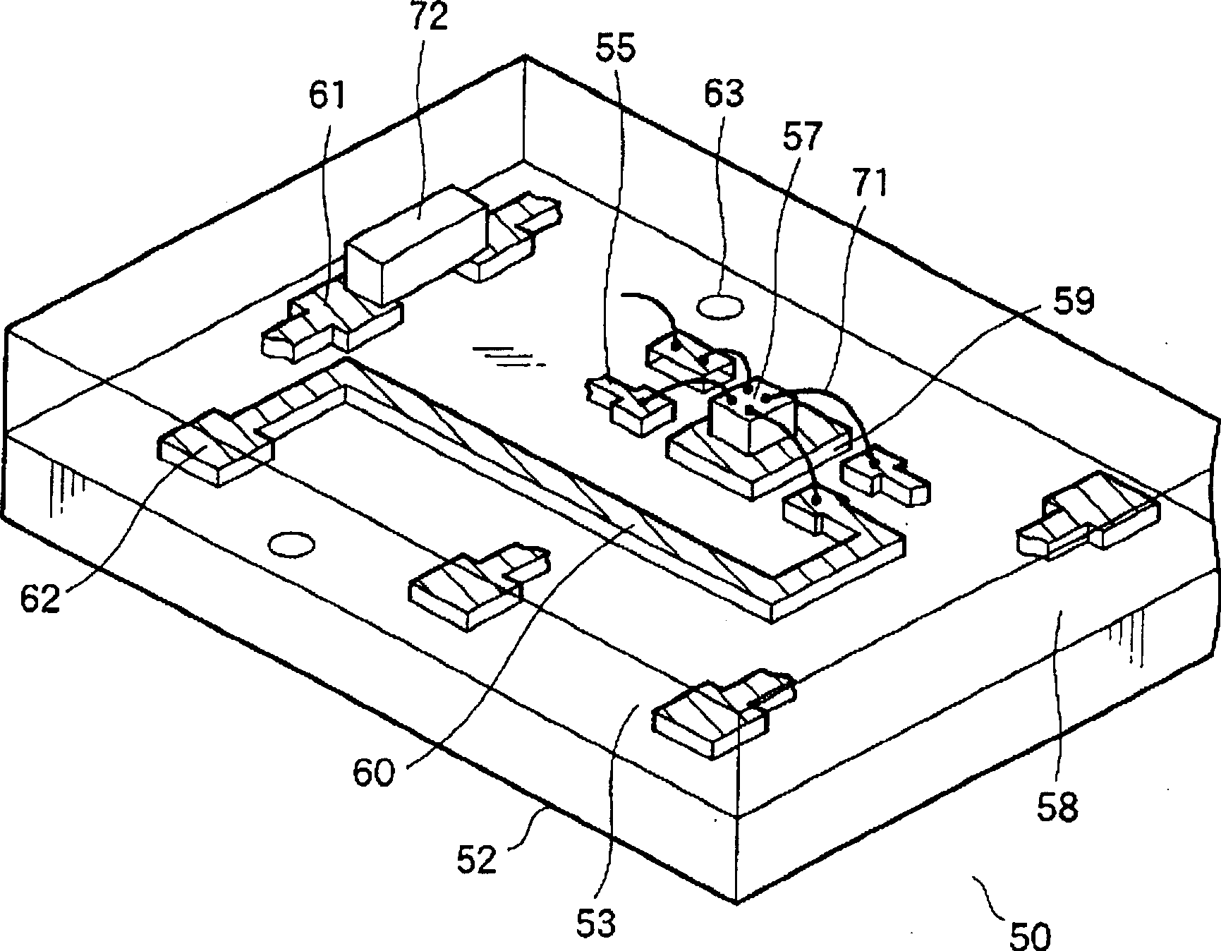
[0099] Figure 1A It is a plate-shaped body showing that a thinner package with better reliability during miniaturization can be realized than a conventional IC or a hybrid IC using a standard frame.

[0100] The plate-shaped body 50, such as Figure 1A The pattern of its conventional hybrid IC is formed by a conductive cover film 56 as shown.

[0101] That is, the plate-shaped body 50 has a first surface 52 formed of a flat surface, and a second surface 53 formed of a flat surface provided to face the first surface 52 .

[0102] On the second surface 53, a first conductive cover film 56 having substantially the same pattern as the plurality of first pads 55 provided on or near the semiconductor element mounting region 54 is formed.

[0103] The plate-shaped body 50 may be formed with an etching-resistant mask such as photoresist instead of the aforementioned conductive coating. At this time, at least the ...


PUM


Abstract

In the present invention there is formed a sheet-like board member 50 having conductive coating films, such as first pads 55 and die pads 59, formed thereon or a sheet-like board member 50 which has been half-etched by using conductive coating films such as first pads 55 and die pads 59. A hybrid IC can be manufactured by means of utilization of post-processing processes of a semiconductor manufacturer. Further, a hybrid IC can be manufactured without adoption of a support board, and hence there can be manufactured a hybrid IC which is of lower profile and has superior heat dissipation characteristics.

Description

technical field [0001] The present invention relates to a plate-like body and a method of manufacturing a semiconductor device, and more particularly, to a plate-like body that solves various problems of conventional hybrid ICs. Background technique [0002] Conventionally, circuit devices incorporated in electronic equipment have been required to be miniaturized, thinned, and lightweight for use in cellular phones, portable computers, and the like. [0003] As the circuit device, a multi-purpose hybrid IC is used, and as the base, a ceramic base, a metal base, a printed circuit board or a flexible base is mainly used. [0004] Figure 17 It is a figure which shows an example, and the concrete structure is demonstrated below. [0005] First, there is the aforementioned bottom plate 1 on which conductive patterns are formed using Cu. The conductive pattern is a chip pad 2, a connection pad 3, an electrode 4 for external lead-out, a fixed pad 5 for co...

Claims


Application Information

Patent Timeline
Patent Type & Authority Patents(China)
IPC IPC(8): H01L23/48H01L21/60H05K1/18H05K3/30H01L25/18H01L21/48H01L21/56H01L21/68H01L21/98H01L23/495H01L23/50H01L25/04
CPCH01L2924/0105H01L2224/97H01L2224/0401H01L2924/19041H01L2924/01028H01L2224/48091H01L2924/01083H01L2224/49171H01L2924/01013H01L24/49H01L25/50H01L24/45H01L24/06H01L2924/19043H01L24/48H01L2224/48247H01L2924/01033H01L21/4832H01L2924/01078H01L2924/13055H01L2924/01015H01L2924/01023H01L2924/19105H01L2924/01046H01L2221/68377H01L2924/01082H01L2924/01004H01L21/566H01L2224/32245H01L2924/01002H01L2924/01029H01L2924/01087H01L2224/05556H01L2224/48464H01L2924/014H01L2924/18301H01L24/97H01L23/49541H01L23/49575H01L2224/48599H01L2924/01047H01L2224/48137H01L2924/01079H01L24/05H01L2924/19107H01L2224/48227H01L2224/04042H01L2924/14H01L2924/01005H01L2924/01006H01L2924/01014H01L2924/01058H01L2224/45144H01L2224/73265H01L21/561H01L21/565H01L2224/05554H01L2924/15787H01L2924/181H01L2924/00014H01L2224/85H01L2224/83H01L2924/00H01L2924/00012H01L23/48Y10T29/4913Y10T29/49128
Inventor 坂本则明小林义幸阪本纯次真下茂明大川克实前原荣寿高桥幸嗣
Owner SANYO ELECTRIC CO LTD
Why Eureka
Try Eureka