

Öä
A carbon nanotube and logic technology, applied in the field of micro-nano electronic device circuits, can solve the problems of complex structure and difficult fabrication, and achieve the effects of improving performance and reliability, reducing fabrication difficulty, and reducing gate area
- Summary
- Abstract
- Description
- Claims
- Application Information
AI Technical Summary
Problems solved by technology
Method used
Image

Examples
Embodiment 1
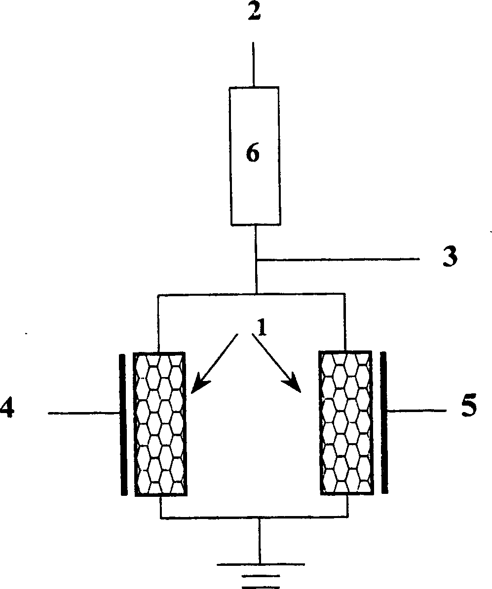
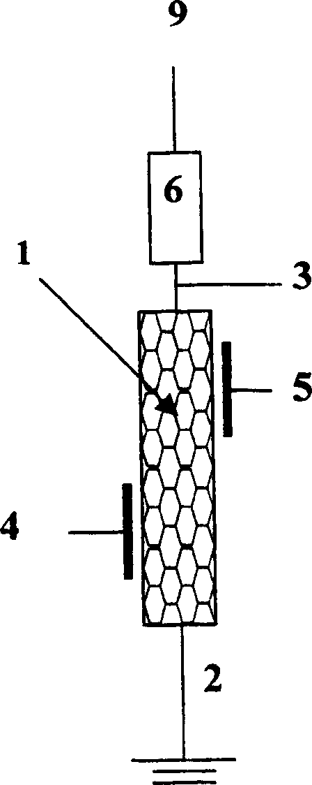
[0056] according to image 3 , 4 and 5 make the "OR" gate logic device of the carbon nanotube double gate structure of the utility model.
[0057] Silicon with (001) orientation is selected as the substrate 11 . Utilize organic vapor phase deposition method (PECVD), prepare the SiO with 300nm thick on the substrate 11 2 Layer 10. First make the gate 4, 5: in SiO 2 Electron photoresist (PMMA) with a thickness of 80 nm is uniformly coated on the insulating layer 10 . The photoresist after electron beam exposure is developed and fixed, and after the exposed photoresist is removed, two grooves with a width of 30 nm and a distance of 50 nm are formed on the photoresist layer. Etching of SiO without photoresist coverage using dry etching 2 , in SiO 2 Two trenches with a width of 30nm, a depth of 30nm and a distance of 50nm are formed on the insulating layer. A layer of Al with a thickness of 30 nm is deposited on the entire surface of the device by electron beam evaporation....
Embodiment 2
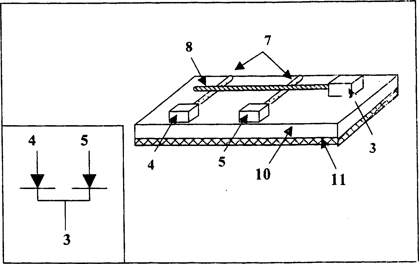
[0059] according to image 3 , 5 and 6 make another "OR" gate logic device with carbon nanotube double gate structure of the present utility model.
[0060] Silicon with (001) orientation is selected as the substrate 11 . Utilize organic vapor phase deposition method (PECVD), prepare the SiO with 300nm thick on the substrate 11 2 Layer 10. First make the gate 4, 5: in SiO 2 Electron photoresist (PMMA) with a thickness of 80 nm is uniformly coated on the insulating layer 10 . The photoresist after electron beam exposure is developed and fixed, and after the exposed photoresist is removed, two grooves with a width of 30 nm and a distance of 50 nm are formed on the photoresist layer. Etching of SiO without photoresist coverage using dry etching 2 , in SiO 2 Two trenches with a width of 30nm and a depth of 30nm are formed on the insulating layer. A layer of Al with a thickness of 30 nm was deposited on the entire device surface by electron beam evaporation. The photoresis...
PUM
 Abstract
Description
Claims
Application Information