

Semiconductor device
A semiconductor and component technology, applied in the field of semiconductor components, to achieve the effect of reducing inactive current and suppressing substrate current
- Summary
- Abstract
- Description
- Claims
- Application Information
AI Technical Summary
Problems solved by technology
Method used
Image

Examples
Embodiment Construction
[0039] Embodiments of the present invention will be described below with reference to the drawings. The embodiments do not limit the present invention.
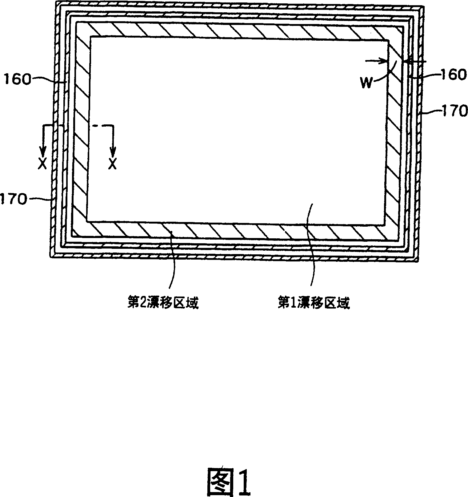
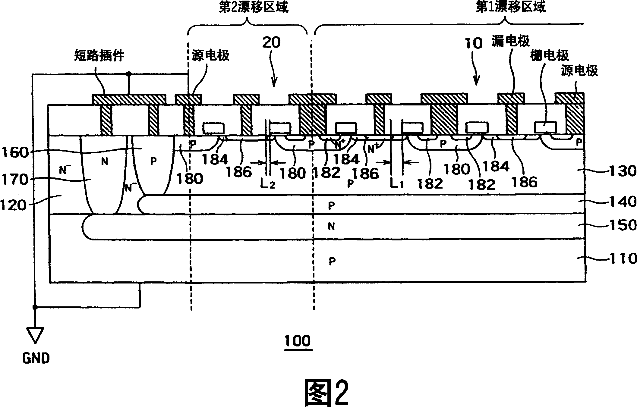
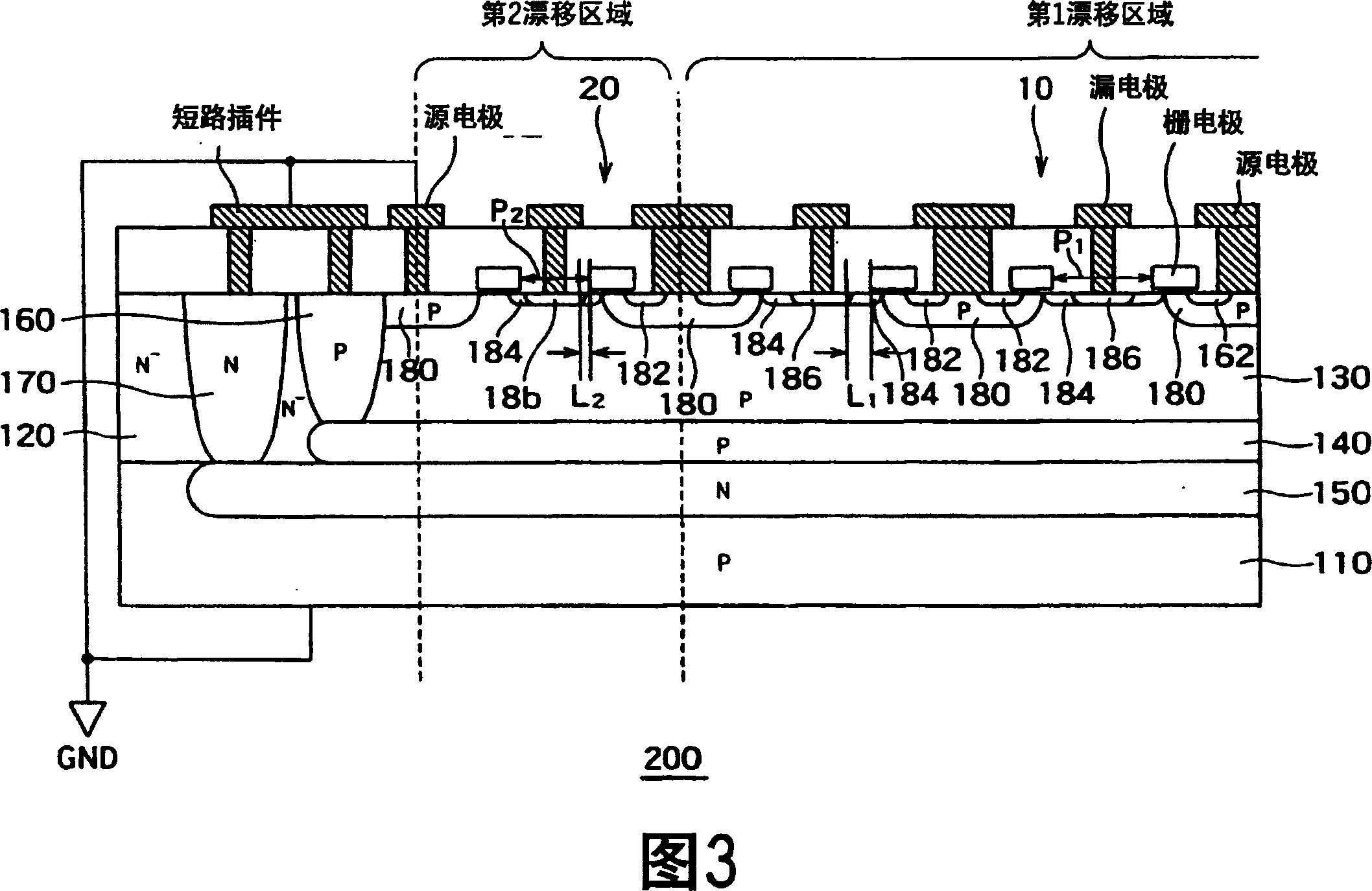
[0040] FIG. 1 is a top view of an LDMOS region according to an embodiment of the present invention. This LDMOS region is divided into a first drift region and a second drift region. The second drift area is provided around the first drift area. The P-type connection region 160 is provided around the second drift region. Also, an N-type connection region 170 is disposed around the connection region 160 . Peripheral logic circuits (not shown) such as a control circuit for controlling LDMOS are provided around the connection region 170 .
[0041] The second drift region is sandwiched between the first drift region and the connection region 160 in any of the planar regions shown in FIG. 1 . That is, the second drift region is closer to the connection region 160 than the first drift region.
[0042] 2 to 6 are enlarged cross...
PUM
 Abstract
Description
Claims
Application Information