Eureka AIR delivers breakthrough ideas for toughest innovation challenges, trusted by R&D personnel around the world.

Field emitting cathode and its making process and application

A technology of field emission cathode and manufacturing method, which is applied in cold cathode manufacturing, electrode system manufacturing, discharge tube/lamp manufacturing, etc., can solve problems such as limiting technology application, and achieve strong field emission capability, high intensity, and low field strength Effect

Inactive Publication Date: 2002-05-15
PEKING UNIV
View PDF0 Cites 27 Cited by
  • Summary
  • Abstract
  • Description
  • Claims
  • Application Information

AI Technical Summary

Problems solved by technology

The deficiencies of the above technologies limit the application of each technology

Method used


Image

  • Field emitting cathode and its making process and application
  • Field emitting cathode and its making process and application
  • Field emitting cathode and its making process and application

Examples


Embodiment 1

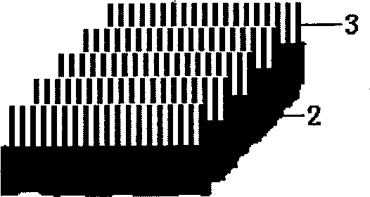
[0036] Such as figure 1 Shown is a schematic structural view of the field emission cathode of the present invention—a metal nanowire array. The nanopore templates used in fabrication have been dissolved away. Metal nanowires 3 of the same metal as the base metal film 2 are grown on the base metal film 2 , which is the base of the metal planar electrode, and the metal nanowires 3 are arranged in an array. Embodiment 2: Utilize the electrochemical deposition method to manufacture metal nanowire arrays

Embodiment 2

[0036] Such as figure 1 Shown is a schematic structural view of the field emission cathode of the present invention—a metal nanowire array. The nanopore templates used in fabrication have been dissolved away. Metal nanowires 3 of the same metal as the base metal film 2 are grown on the base metal film 2 , which is the base of the metal planar electrode, and the metal nanowires 3 are arranged in an array. Embodiment 2: Utilize the electrochemical deposition method to manufacture metal nanowire arrays

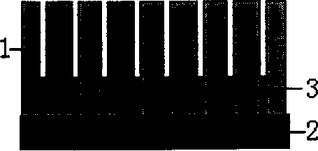
[0037] Such as figure 2 As shown, the selected metal is gold (Au), the selected nanopore template 1 is a polycarbonate template with a pore diameter of 30 nanometers (nm) and a thickness of 2 micrometers (μm), and the positions of the nanopores are randomly distributed. Vacuum deposit a 200 nanometer (nm) thick gold (Au) film on one side of the template, and then electroplate gold (Au) or copper (Cu) to a thickness of 10 microns (μm) to form a base metal film 2 as a field emi...

Embodiment 3

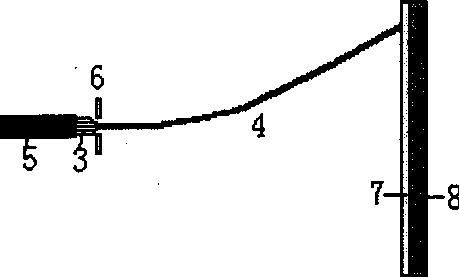
[0041] Such as image 3 Shown is a schematic diagram of the structure of the field emission cathode of the present invention—a metal nanowire array used as a cold cathode electron source for a cathode ray tube (CRT). The metal nanowire 3 is used as the electron source of the cathode 5 , and the electron beam 4 emitted by it is controlled by the grid 6 and emitted to the fluorescent screen 7 , which is placed in the glass envelope 8 .


PUM

PropertyMeasurementUnit
Thicknessaaaaaaaaaa
Diameteraaaaaaaaaa
Lengthaaaaaaaaaa

Abstract

The invention field emitting cathode is a metal nano wire array which grows on metal base of planar electrode and the metal is same as the base's. The thickness of base is 1 micro m to 0.5 mm, the diameter of nano wire is 20-200 nm, the length is 100 to 500 nm. The producing steps are: to select modular board with nanometer holes according to size requirement of display unit, to make a metal filmelectrode on a surface of the selected modular board by evaporating and electroplating, to electrochemical grow metal nanometer wire array in the nanometer holes of nanometer modular board, to clean and dry the dissolved part or whole modular to expose metal nanometer wires. It can be used to cathode-ray tube and plate display, and has low beginning field strength for field emitting cathode, highcurrent density and low cost.

Description

Technical field: [0001] The invention belongs to the field of nanotechnology and the field of planar field emission cathode technology. Background technique: [0002] Existing planar field emission cathodes generally include: silicon tip arrays, carbon nanotube arrays, vapor phase diamond films, and the like. The silicon tip array field emission cathode is based on microelectronics processing technology, with large tip size, low tip density, poor consistency, low resolution, high technical difficulty, low yield and high cost. Carbon nanotube arrays have the same problems as silicon tip arrays if photolithography is used, but carbon nanotube films have many impurities, poor repeatability, and unstable performance. However, the nanocrystalline diamond thin film is based on the electron emission of negative electron affinity, and the mechanism and technology are not mature, and a lot of research is still needed. The deficiencies of the above-mentioned technologies limit the a...

Claims


Application Information

Patent Timeline
IPC IPC(8): H01J1/304H01J9/02
Inventor 薛增泉张葵张耿民余宁侯士敏申志勇刘惟敏赵兴钰陈清吴锦雷张兆祥彭练矛
Owner PEKING UNIV
Why Eureka
Eureka Blog
Learn More