Semiconductor memory unit and array using ultra-thin medium breakdown phenomenon

A technology for memory cells and memory arrays, applied in the field of non-volatile programmable semiconductor memory cells and memory arrays, can solve problems such as breakdown of gated diodes, and achieve the effects of improving integration density, reducing manufacturing costs, and shortening development time.

Inactive Publication Date: 2002-05-29
彭泽忠
View PDF5 Cites 10 Cited by
  • Summary
  • Abstract
  • Description
  • Claims
  • Application Information

AI Technical Summary

Problems solved by technology

Thereafter, when the gated diode is read

Method used


Image

  • Semiconductor memory unit and array using ultra-thin medium breakdown phenomenon
  • Semiconductor memory unit and array using ultra-thin medium breakdown phenomenon
  • Semiconductor memory unit and array using ultra-thin medium breakdown phenomenon

Examples


Embodiment Construction

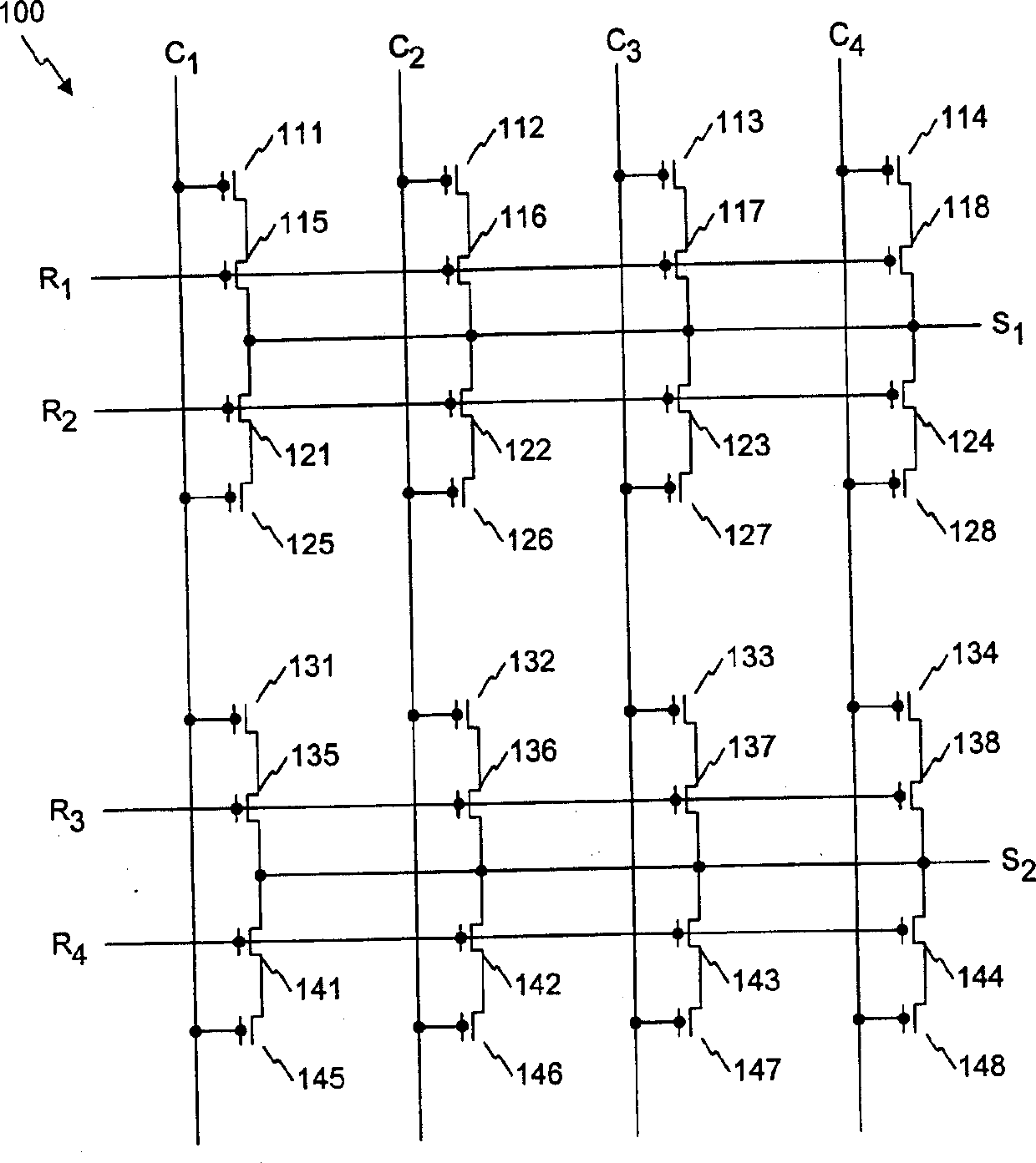
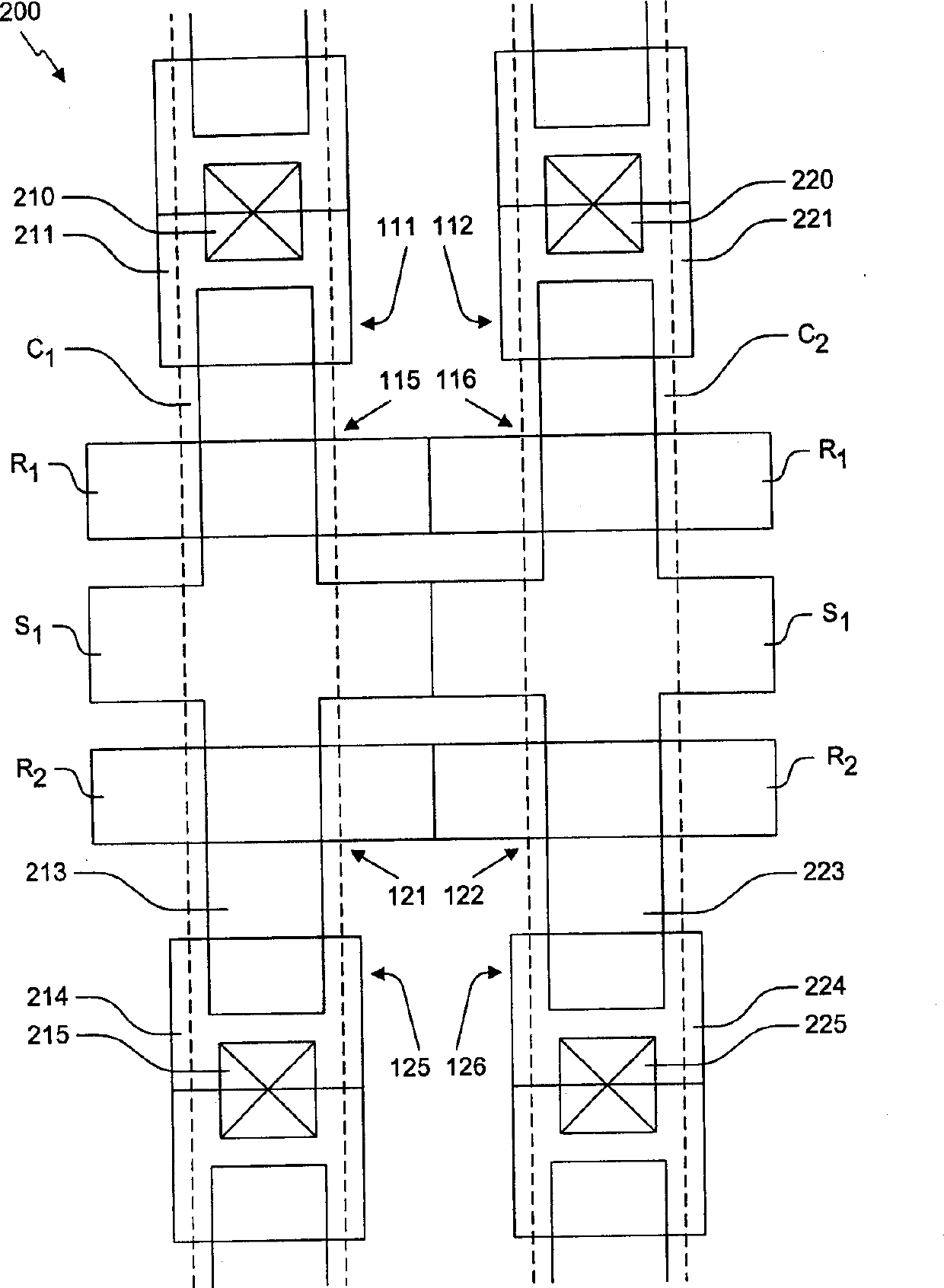
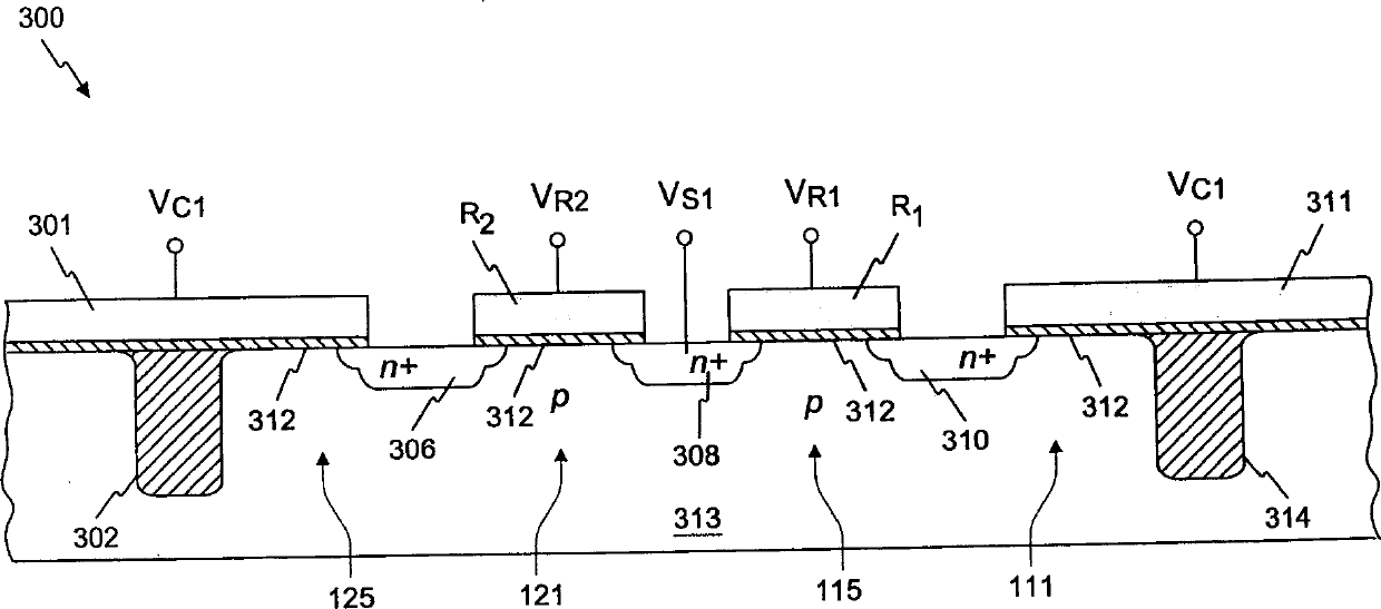
[0072] A semiconductor memory cell with a data storage element formed around an ultra-thin medium (such as a gate oxide layer) is used to store information. The operation method is to stress the ultra-thin medium to cause breakdown (soft breakdown or hard breakdown) ) To establish the leakage current level of the memory cell. The memory cell is read by detecting the current absorbed by the cell. A suitable ultra-thin dielectric is, for example, a high-quality gate oxide layer with a thickness of about 50 angstroms or less. This kind of ultra-thin oxide dielectric is usually used in today's advanced CMOS logic processes. The usual methods for forming this oxide layer include deposition, oxygen growth of silicon active regions, or a combination thereof. Other suitable dielectrics include oxide-nitride-oxide composite dielectrics, compound oxides and so on.

[0073]The following description gives a lot of specific details in order to have a thorough understanding of the present inven...


PUM

PropertyMeasurementUnit
Thicknessaaaaaaaaaa

Abstract

A semiconductor memory unit and memory array based on the breakdown phenomenon of ultra-thin (50 A or less) medium is disclosed. A data storage element around an ultra-thin medium layer (grid oxidizing layer) is made up for storing information. Its method is to apply a stress to said ultra-thin medium to break it down, so creating the leakage current level of memory unit. Its read-out is by sensing the current sucked by the unit. It is made up by advanced CMOS logic technology.

Description

Technical field [0001] The content of the present invention relates to a non-volatile programmable semiconductor memory, more specifically, a non-volatile programmable semiconductor memory cell that uses an ultra-thin medium (such as a MOS gate medium) to store digital information and a memory array using such a cell. Background technique [0002] The non-volatile memory can retain the stored data even after the power is removed. This is necessary or at least highly desirable in many different kinds of computers and other electronic devices. A common type of non-volatile memory is Programmable Read-Only Memory ("PROM"), which utilizes word line / bit line intersection elements such as fuses and anti-fuse and avalanche injection of metal oxides such as floating gate A charge trap device such as a semiconductor ("FAMOS") transistor is used to store logic information. PROM is generally not reprogrammable. [0003] A PROM cell that uses the breakdown of the s...

Claims


Application Information

Patent Timeline
IPC IPC(8): G11C11/34G11C16/00H01L27/105H01L27/115
Inventor 彭泽忠
Owner 彭泽忠
Why Eureka
Try Eureka