Method for producing electrophoretic microchip
A production method and microchip technology, applied in the direction of material analysis, measuring devices, instruments, etc. through electromagnetic means, can solve the problems of unclear surface characteristics, low temperature resistance, difficulty in bonding quartz glass, etc., and meet the technological conditions Easy to meet, flat inner wall, simplified sintering process
- Summary
- Abstract
- Description
- Claims
- Application Information
AI Technical Summary
Problems solved by technology
Method used
Image
Examples
Embodiment 1
[0050] Example 1 Single lane capillary electrophoresis microchip
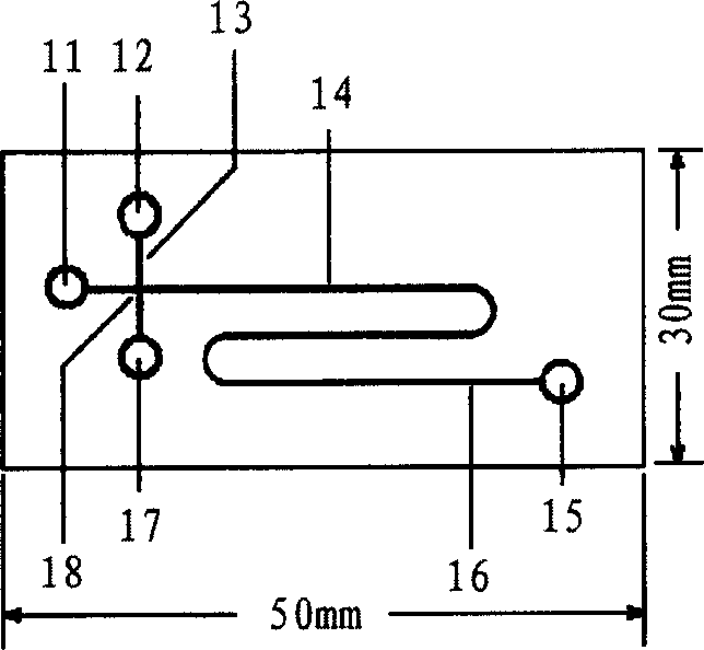
[0051] Consider the following parameters when designing the chip: the width and length of the injection lane and the separation lane, the shape of the injection lane and the separation lane, etc. The pipeline graphics in this example are as follows: image 3 shown. Make the designed pipeline pattern into a mask plate for further photolithographic transfer to the substrate.
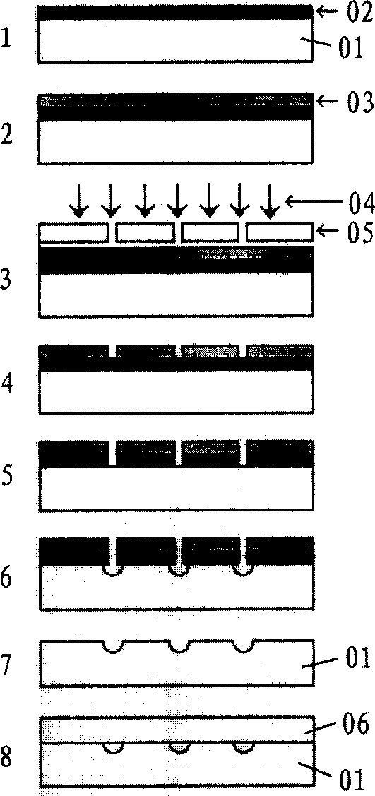
[0052] The fabrication process of electrophoretic microchips such as figure 1 shown, including the following steps:
[0053](1) Cut the quartz sheet into a certain size such as 5cm×3cm according to the requirements. After cleaning, use N 2 Air-dried, pre-baked at 80°C for 10 minutes; after that, a layer of metal chromium was plated on the surface as a sacrificial layer 02 ( figure 1 step 1);
[0054] (2) Then apply a layer of photoresist 03 (Positive Resist #1813) on the glue machine, rotate at 3000 rpm, bake at 80°C for 15 minutes (...
Embodiment 2
[0061] Example 2 Multi-lane array capillary electrophoresis microchip
[0062] Consider the following parameters during the design of the multi-lane array capillary electrophoresis microchip made in this embodiment: the number of swimming lanes, the layout of the swimming lanes, the length and width of the swimming lanes, the spacing and shape of the swimming lanes, and the reasonable distribution of the liquid storage tanks, etc., design graphics such as Figure 5 shown. Make the designed pipeline pattern into a mask plate for further photolithographic transfer to the substrate.
[0063] The manufacturing process is the same as in Embodiment 1, and the completed chip is as follows: Image 6 shown.
PUM
 Abstract
Description
Claims
Application Information


