
Optical storage medium containing unordered nano composite film and its application

An optical storage medium and nanocomposite technology, applied in its application field in optical discs, can solve the problems that the surface roughness of the crystallization state has a great influence on the performance, low light transmittance, low excitation efficiency, etc.

Inactive Publication Date: 2003-02-05
TSINGHUA UNIV
View PDF0 Cites 0 Cited by
  • Summary
  • Abstract
  • Description
  • Claims
  • Application Information

AI Technical Summary

Problems solved by technology

[0004] However, the SiN (170nm) / Sb (15nm) / SiN (20nm) structure also has the following problems: (1) the melting point of the Sb film is low and the thermal stability is poor; (2) the light transmittance of the Sb film is low (generally 10 %~20%), the loss of light energy is large; (3) The crystallization status and surface roughness of the Sb film have a great influence on the performance, which is not conducive to the stability of production and the repeatability of performance; (4) non-metallic / metallic The excitation of the surface plasmon wave on the (or semi-metal) interface is related to the incident direction of the light. Only the part of the light in the focused beam that is greater than the critical angle will contribute to the plasma excitation, the excitation efficiency is low, and the optical system is required Has a large numerical aperture

Method used


Image

  • Optical storage medium containing unordered nano composite film and its application
  • Optical storage medium containing unordered nano composite film and its application
  • Optical storage medium containing unordered nano composite film and its application

Examples


Embodiment 1

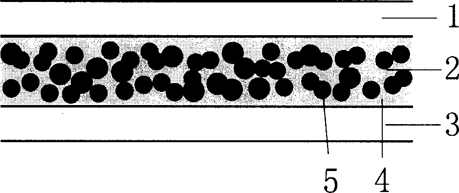
[0022] Both the first and second spacer layers are Si 3 N 4 , and the thicknesses are 170nm and 50nm respectively; the disordered nanocomposite film structure layer is made of Si 3 N 4 and Sb, the volume fraction of Sb in this example is 0.66; the size of the particles is 20nm, and the Sb particles are dispersed in Si 3 N 4 In the matrix, the film thickness is 150 nm, and the transmittance T=53.08%.

Embodiment 2

[0024] The materials of the first and second spacer layers and the composition of the disordered nanocomposite thin film structure layer are the same as in Example 1. The volume fraction of Sb is 0.5; the particle size is 10 nm, and the film thickness is 50 nm. The thicknesses of the first and second spacer layers are respectively 50 nm and 20 nm in sequence. Transmittance T=70.57%.

Embodiment 3

[0026] The materials of the first and second spacer layers and the composition of the disordered nanocomposite thin film structure layer are the same as in Example 1. The volume fraction of Sb is 0.33; the particle size is 0.5 nm, and the film thickness is 10 nm. The thicknesses of the first and second spacer layers are respectively 20 nm and 0 nm in turn. Transmittance T=87.13%.


PUM

PropertyMeasurementUnit
diameteraaaaaaaaaa
thicknessaaaaaaaaaa
thicknessaaaaaaaaaa

Abstract

The invented optical storage media of the disorder nano composite film as well as the application belongs to the optical memory technique area. The media includes the first interval layer, the second layer and the structural layer of the disorder nano composite film between the first and second layers. The composite film contains the following components: the insulator with good transparency of the semiconductor with the wide energy gap as well as any one or more kinds of metal, semi-metal or semiconductor with the volume fraction 0.3-0.7. The two components are random distributed. The invention also discloses the structure of the erasable and read only optical disc made from the said media. The media possesses the effects of light amplification and super diffraction resolution so as to realize the super high-density optical storage with the features of high thermal stability, good transmittance, etc.

Description

technical field [0001] An optical storage medium containing disordered nanocomposite films belongs to the optical storage medium manufacturing technology, and also relates to its application in optical discs. Background technique [0002] The use of near-field optical methods in optical storage can overcome the limitation of the diffraction limit and greatly increase the optical storage capacity. Early near-field optical storage schemes mainly use optical probes to record in the range of the optical near-field. The disadvantage is that the nanoscale flight height between the optical probe and the optical disc is not easy to measure and control. In 1998, Tominaga et al proposed that a sandwich structure - SiN(170nm) / Sb(15nm) / SiN(20nm) - could be used to conveniently realize near-field ultra-high density optical storage. This sandwich-type super-diffraction-resolved near-field structure can be applied not only in the field of optical storage, but also in other fields that nee...

Claims


Application Information

Patent Timeline
Patent Type & Authority Applications(China)
IPC IPC(8): G11B7/257G11B11/24
Inventor 区定容朱静王佳朱若剑赵嘉昊周惠华
Owner TSINGHUA UNIV
Learn More