

Light-emitting device
A technology of light-emitting elements and barrier layers, applied in electrical components, laser parts, lasers, etc., can solve problems such as poor surface state, and achieve the effect of improving crystallinity
- Summary
- Abstract
- Description
- Claims
- Application Information
AI Technical Summary
Problems solved by technology
Method used
Image

Examples
Embodiment approach 1
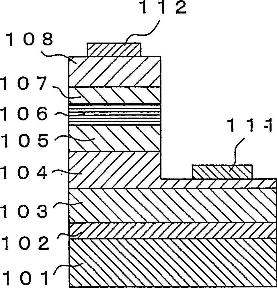
[0047] figure 1 It is a model structure showing Embodiment 1 in which the present invention is applied to a light emitting diode. In the light emitting diode according to Embodiment 1, a buffer layer 102, an undoped GaN layer 103, an n-type contact layer 104, an n-type cladding layer 105, an active layer 106, and a p-type cladding layer 107 are sequentially stacked on a substrate 101. , and a p-type contact layer 108, and an n-electrode 111 and a p-electrode 112 are formed on the n-type contact layer 104 and the p-type contact layer 108, respectively.
[0048] The substrate 101 is used to grow a desired nitride semiconductor layer (In x Al y Ga 1-x-y N, x≥0, y≥0, x+y≤1) can be appropriately selected. The buffer layer 102 is to relax the substrate 101 and the nitride semiconductor (In x Al y Ga 1-x-y N, x≥0, y≥0, x+y≤1) The lattice constant is not positive and the layer formed. The undoped GaN layer 103 is formed to improve the crystallinity of the n-type contact layer ...
Embodiment approach 2
[0084] Next, a light emitting diode according to Embodiment 2 of the present invention will be described.
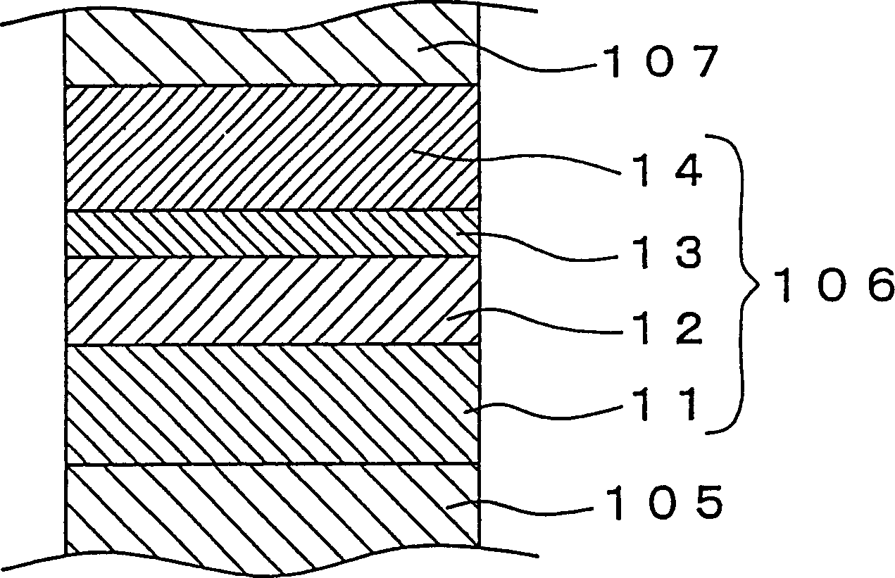
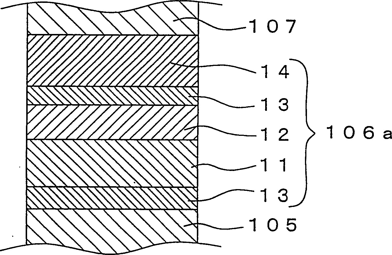
[0085] As described above, the present invention is very suitable for a multiple quantum well structure because it can improve the crystallinity of layers formed above the well layer 12 and the first barrier layer 13 .
[0086] That is, the light-emitting element according to Embodiment 2 of the present invention adopts Figure 5 The illustrated light-emitting diode has the same structure as that of the first embodiment except that the active layer 106c of the multiple quantum well structure is used instead of the active layer 106 of the light-emitting element of the first embodiment.
[0087] In the light-emitting element of Embodiment 2, if Figure 5 As shown, the active layer 106c of the multiple quantum well structure repeatedly forms the second barrier layer 11, the well layer 12, and the first barrier layer 13 in sequence. In this case, the uppermost layer 14 is fo...
Embodiment approach 3
[0096] Hereinafter, a light-emitting element according to Embodiment 3 of the present invention in which the present invention is applied to a laser element will be described.
[0097] Figure 8 It is a schematic diagram showing the structure of a nitride semiconductor laser element as a light emitting element according to the third embodiment.
[0098] In the nitride semiconductor laser element of Embodiment 3, a buffer layer 202, an n-type contact layer 203, an n-type cladding layer 204, an n-type light guiding layer 205, an active layer 206, and a p-type light guiding layer are sequentially stacked on a substrate 201. Layer 207 , p-type cladding layer 208 , p-type contact layer 209 , and n-electrode 211 and p-electrode 212 are respectively formed on n-type cladding layer 204 and p-type cladding layer 208 .
[0099] The configuration of the substrate 201 , the buffer layer 202 , the n-type contact layer 203 , and the n-type cladding layer 204 is the same as that of the firs...
PUM
| Property | Measurement | Unit |
|---|---|---|
| Film thickness | aaaaa | aaaaa |
Abstract
Description
Claims
Application Information