Improved structure of circuit anti-interference device

An anti-interference device and circuit technology, applied in printed circuits, printed circuit manufacturing, electrical components, etc., can solve problems such as cracks, affect the accuracy of the test, and do not meet the economic cost efficiency, achieve proper design, and improve the pass rate. , the effect of saving material and labor costs

Inactive Publication Date: 2003-04-30
CAMEO COMM
View PDF0 Cites 3 Cited by
  • Summary
  • Abstract
  • Description
  • Claims
  • Application Information

AI Technical Summary

Problems solved by technology

[0002] According to the general prior art, the design plan of the circuit board 1 is usually provided with several oscillation sources 11 of different frequencies to provide oscillation signals of different frequencies according to various requirements. In general wireless transmission, the transmission carrier is generally a high-frequency signal. When the receiving circuit module receives the high-frequency signal, it is often necessary to convert the high-frequency signal into an intermediate frequency or low-frequency signal to meet the required adjustment signal, wherein the high-frequency signal is mixed in a mixer corresponding to Oscillating source 11, to convert high-frequency signals into different intermediate frequency or low-frequency signals as required; however, in the process of mixing in the mixer, the oscillation sources 11 of different frequency properties often cause mutual interference with each other , so that the output frequency value of the mixer after mixing produces errors. Therefore, someone covers each oscillation source 11 with a cover 12 to isolate the mutual interference between the oscillation sources 11.
[0003] However, the above-mentioned isolation structure needs to be tested for the function of the electrical components before the one or more oscillation sources 11 can be individually isolated. Slight interference affects the accuracy of the test (i.e. causes the pass rate to drop); in addition, the cover 12 of the isolation structure is individually processed to cover the oscillation source 11 of the existing circuit board 1, so that the manufacturing process A large increase, thus affecting the smooth progress of the operation process, and the cover 12 needs to make molds of various sizes according to the size of the vibration source 11, and then often causes disadvantages such as time-consuming and material consumption in the production process, so it is very unfavorable. It is economical and cost-effective; in addition, the cover 11 is generally welded firmly around the vibration source 12 with a soldering iron, so it is very easy to cause local expansion and deformation of the existing circuit board 1 due to heating in a local area, and even lead to cracks Occurrence, and greatly affect the quality of the circuit, it is difficult for the industry to accept

Method used


Image

  • Improved structure of circuit anti-interference device
  • Improved structure of circuit anti-interference device
  • Improved structure of circuit anti-interference device

Examples


Embodiment Construction

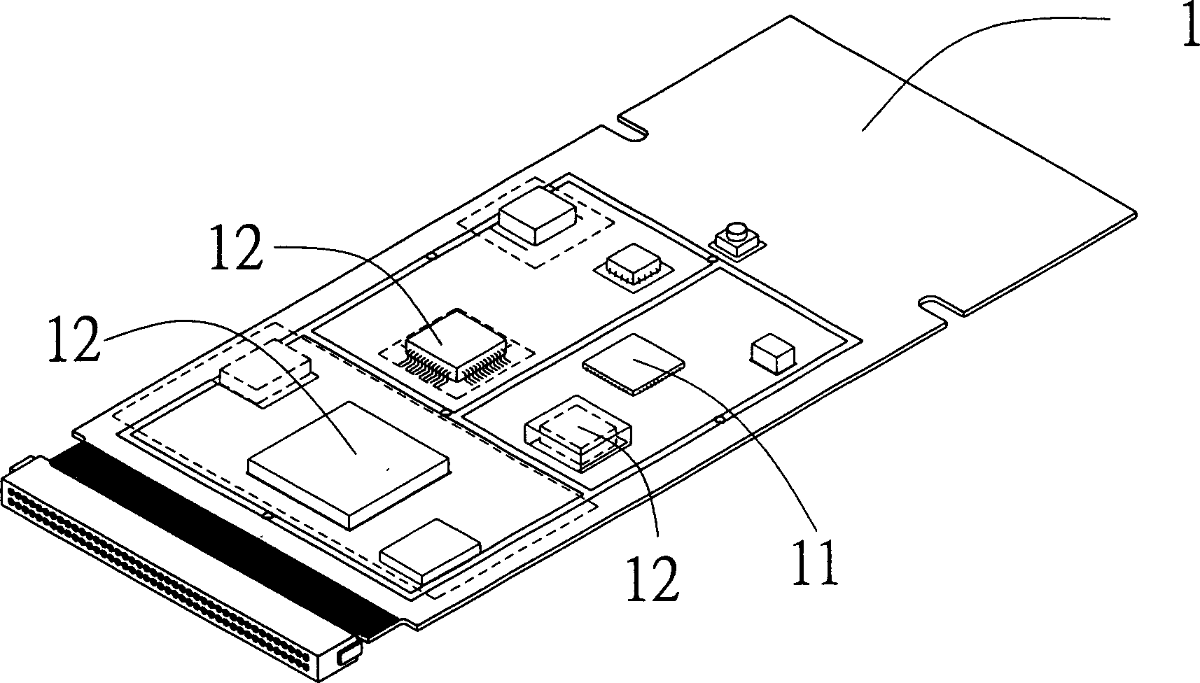
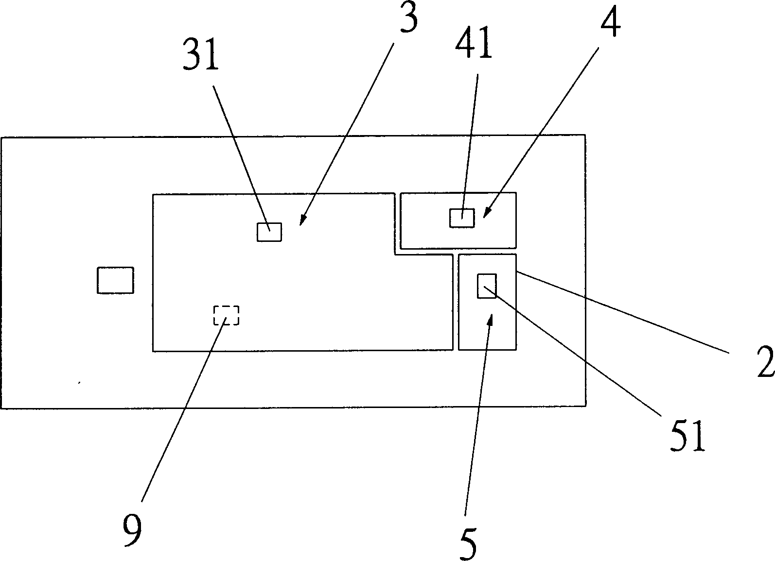
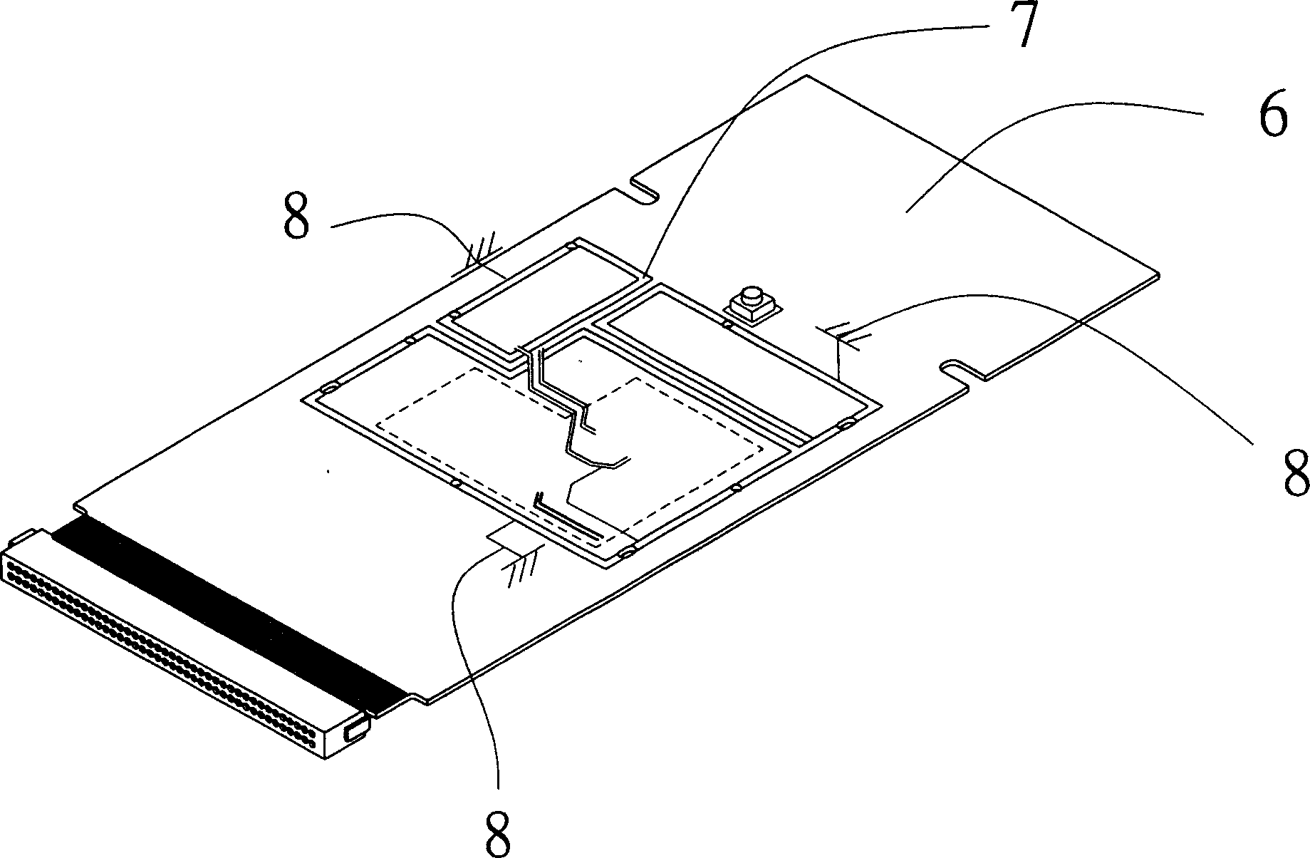
[0022] Such as figure 2 As shown, the present invention is mainly divided into several frequency domain blocks such as high frequency region 3, intermediate frequency region 4 and low frequency region 5 with several frame lines 2 during circuit design, so that each oscillation source (such as: high Frequency oscillation source 31, intermediate frequency oscillation source 41, and low frequency oscillation source 51) belong to the relevant circuit components, each according to the attribute of high or low frequency, each placed in the corresponding frequency domain block, and after the surface treatment operation, that is, in the circuit On the board 6, the pre-divided frequency domain blocks are formed into independent copper wire frames 7 (such as image 3 As shown), with the help of the copper wire frame, the individual signals are respectively introduced into the ground terminal 8, so as to prevent the oscillation sources of different properties (such as: high frequency os...


PUM


Abstract

A structural improvement for antidisturbance device of line uses a number of frame lines to form a number of frequency domain zone blocks according to the requirement by dividing in the design to seteach related circuit element belonging to oscillation source to the fitted frequency domain zone block as per the magnitude of the frequency so that the copper frame body independent to each other being formed on the circuit board by using frequency domain zone blocks divided in advance after the surface being processed with catching. The effective isolation of external impurity message and internal disturbance to each other can be realized by using the copper line frame body to lead the individual / message to the ground end so as to prevent the mixed wave disturbance to each other from oscillation source in different property frequency.

Description

technical field [0001] The invention relates to a line anti-interference device. Background technique [0002] According to the general prior art, the design plan of the circuit board 1 is usually provided with several oscillation sources 11 of different frequencies to provide oscillation signals of different frequencies according to various requirements. In general wireless transmission, the transmission carrier is generally a high-frequency signal. When the receiving circuit module receives the high-frequency signal, it is often necessary to convert the high-frequency signal into an intermediate frequency or low-frequency signal to meet the required adjustment signal, wherein the high-frequency signal is mixed in a mixer corresponding to Oscillating source 11, to convert high-frequency signals into different intermediate frequency or low-frequency signals as required; however, in the process of mixing in the mixer, the oscillation sources 11 of different frequency properti...

Claims


Application Information

Patent Timeline
Patent Type & Authority Applications(China)
IPC IPC(8): H05K3/00H05K9/00
Inventor 林文雄陈逸韬
Owner CAMEO COMM
Why Eureka
Try Eureka