Orgnic electroluminescence device and its preparation device

An electroluminescent device, organic technology, applied in the direction of electroluminescent light source, electro-solid device, semiconductor/solid-state device manufacturing, etc. The effect of low consumption, uniform light emission and high yield

Inactive Publication Date: 2003-05-07
BEIJING VISIONOX TECH
View PDF2 Cites 37 Cited by
  • Summary
  • Abstract
  • Description
  • Claims
  • Application Information

AI Technical Summary

Problems solved by technology

[0004] ① The baking temperature (120°C) of photoresist will damage the organic film;
[0005] ② Solvents, developers, and corrosive solutions of photoresist will damage the organic film;
[0029] Silicon 3 can only be distributed parallel to the direction perpend...

Method used


Image

  • Orgnic electroluminescence device and its preparation device
  • Orgnic electroluminescence device and its preparation device
  • Orgnic electroluminescence device and its preparation device

Examples


Embodiment 1

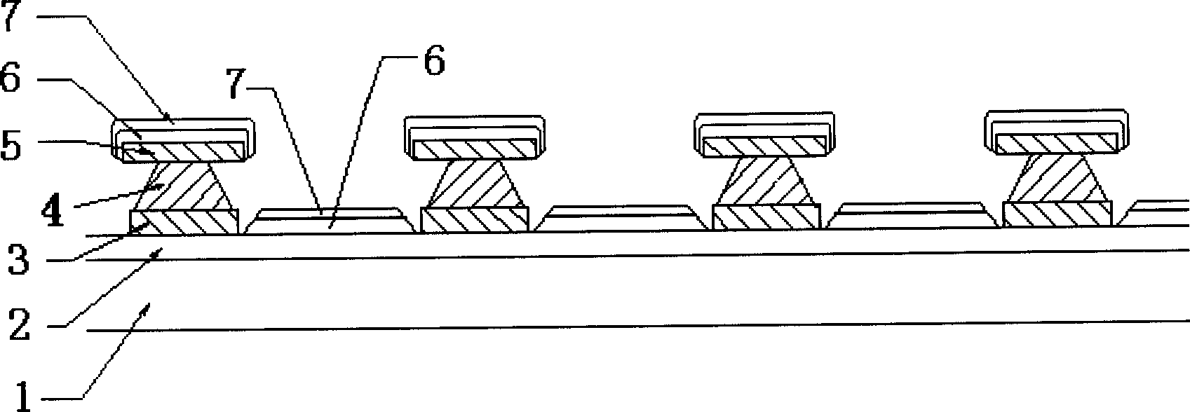
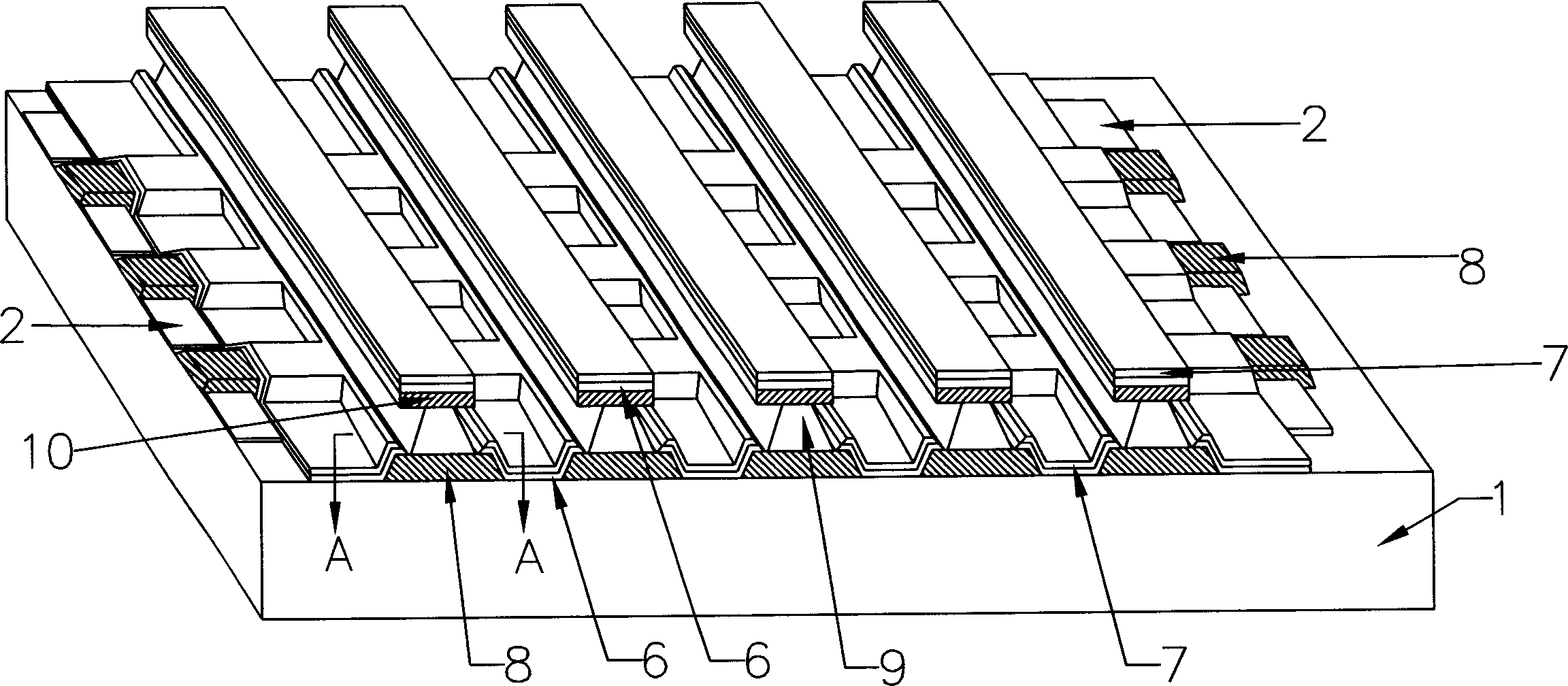
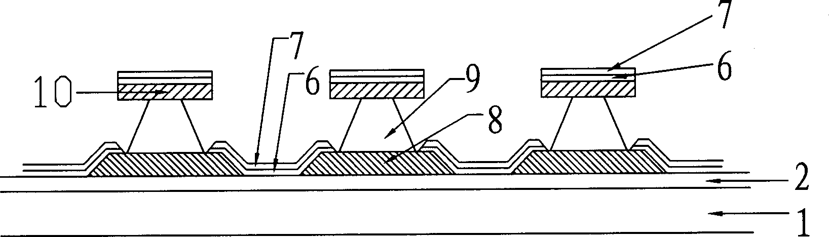
[0104](The entire preparation process of OLEDs is carried out in the purification workshop). The ITO glass with a sheet resistance of 15Ω is ultrasonically cleaned and dried with acetone-ethanol solution (volume ratio 2:1). The ITO film thickness is 170nm. A group of parallel and separated straight lines with a line width of 400 μm were produced. Then, the first layer of insulation material PI for isolation columns is spin-coated with a film thickness of 2 μm. Lithograph PI into a network structure, that is, there are PI lines in the vertical direction to ITO and the parallel direction to ITO (between the ITO lines), and develop in 3% NaOH solution for 30s, so that the cross-section of the lines forms a positive trapezoid with a small top and a large bottom shape, with a line width of 30 μm. Bake in a convection oven at 210° C. for 30 minutes to completely cure the PI. Then continue to spin-coat the second layer of isolation column insulating material PI on this basis, with ...

Embodiment 2

[0106] (The entire preparation process of OLEDs is carried out in the purification workshop). The ITO glass with a sheet resistance of 5Ω is ultrasonically cleaned and dried with acetone-ethanol solution (volume ratio 2:1). The ITO film thickness is 200nm. A group of parallel and separated straight lines with a line width of 200 μm were produced. Then spin-coat the first layer of positive photoresist AZ6112 (Clariant Co., Ltd., Japan) with a film thickness of 0.5 μm. The photolithography forms a network structure, that is, there are positive photoresist lines in the direction perpendicular to the ITO and parallel to the ITO (between the ITO lines), and the positive photoresist developer is used to develop the cross-section of the lines to form a small top and a large bottom. regular trapezoidal shape with a line width of 20 μm. Bake in a convection oven at 220° C. for 30 minutes to completely cure the positive photoresist. Then continue to spin-coat the second layer of isola...

Embodiment 3

[0108] (The entire preparation process of OLEDs is carried out in the purification workshop). The ITO glass with a sheet resistance of 15Ω is ultrasonically cleaned and dried with acetone-ethanol solution (volume ratio 2:1). The ITO film thickness is 170nm. A group of parallel and separated straight lines with a line width of 600 μm were produced. Then spin-coat the first layer of isolation column insulating material photosensitive PI with a film thickness of 1 μm. The photosensitive PI is photolithographically formed into a network structure, that is, there are photosensitive PI lines in the direction perpendicular to the ITO and parallel to the ITO (between the ITO lines), and developed in a dimethylformamide developer for 50 seconds to form a cross-section of the lines. A regular trapezoidal shape with a small top and a large bottom, with a line width of 50 μm. Bake in a convection oven at 220° C. for 30 minutes to completely cure the photosensitive PI. On this basis, con...


PUM


Abstract

The invention belongs to the technique area of the semiconductor elements and devices. Three layers of the isolation pole are prepared on the graphics of the first electrode. The graphics of the first layer of the isolation pole is the mesh texture with the cross section being as trapezoid shape. The cross section of the lines on the second layer and the third layer of the isolation pole possess the shape with big at the upper and small at the lower. Then, the organic function layer and the second electrode are deposited in sequence. The shadow effect caused by the shape with big at the upper of the second layer and the third layer makes the second electrode possible to be partitioned. The first layer of the isolation pole being equivalent to 'insulating base' prevents the short circuit between the electrodes.

Description

technical field [0001] The invention relates to an organic electroluminescence device and a preparation method of the device, belonging to the technical field of electronic semiconductor components. Background technique [0002] Organic Electroluminescent Devices (Organic Electroluminescent Devices, hereinafter referred to as OLEDs) are generally composed of a transparent first electrode located on a transparent substrate, an organic electroluminescent medium (organic functional layer) deposited on the first electrode, and an organic electroluminescent medium (organic functional layer) located on the transparent substrate. The second electrode (metal electrode) above the organic electroluminescence medium. The transparent electrode serves as the anode of the device, and the metal electrode serves as the cathode of the device. Apply a high level to the transparent electrode and a low level to the metal electrode to make the device emit light. A group of anodes (or cathodes)...

Claims


Application Information

Patent Timeline
IPC IPC(8): H01L51/52H01L51/56H05B33/10H05B33/12
Inventor 邱勇杨萍邵玉暄王立铎张德强
Owner BEIJING VISIONOX TECH
Why Eureka
Try Eureka