

Method for manufacturing jet hole piece of ink jet type print head by using microfilm procedure
A manufacturing method and printing head technology, applied in printing and other directions, can solve problems such as expensive, difficult to accurately control process conditions, and costly
- Summary
- Abstract
- Description
- Claims
- Application Information
AI Technical Summary
Problems solved by technology
Method used
Image

Examples
no. 1 example
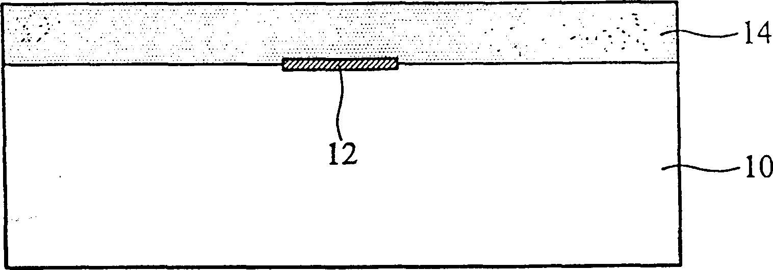
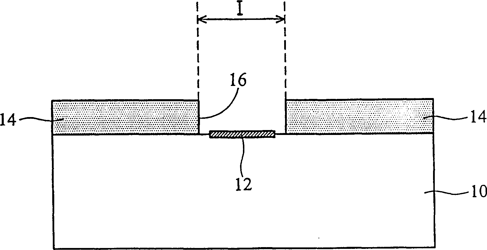
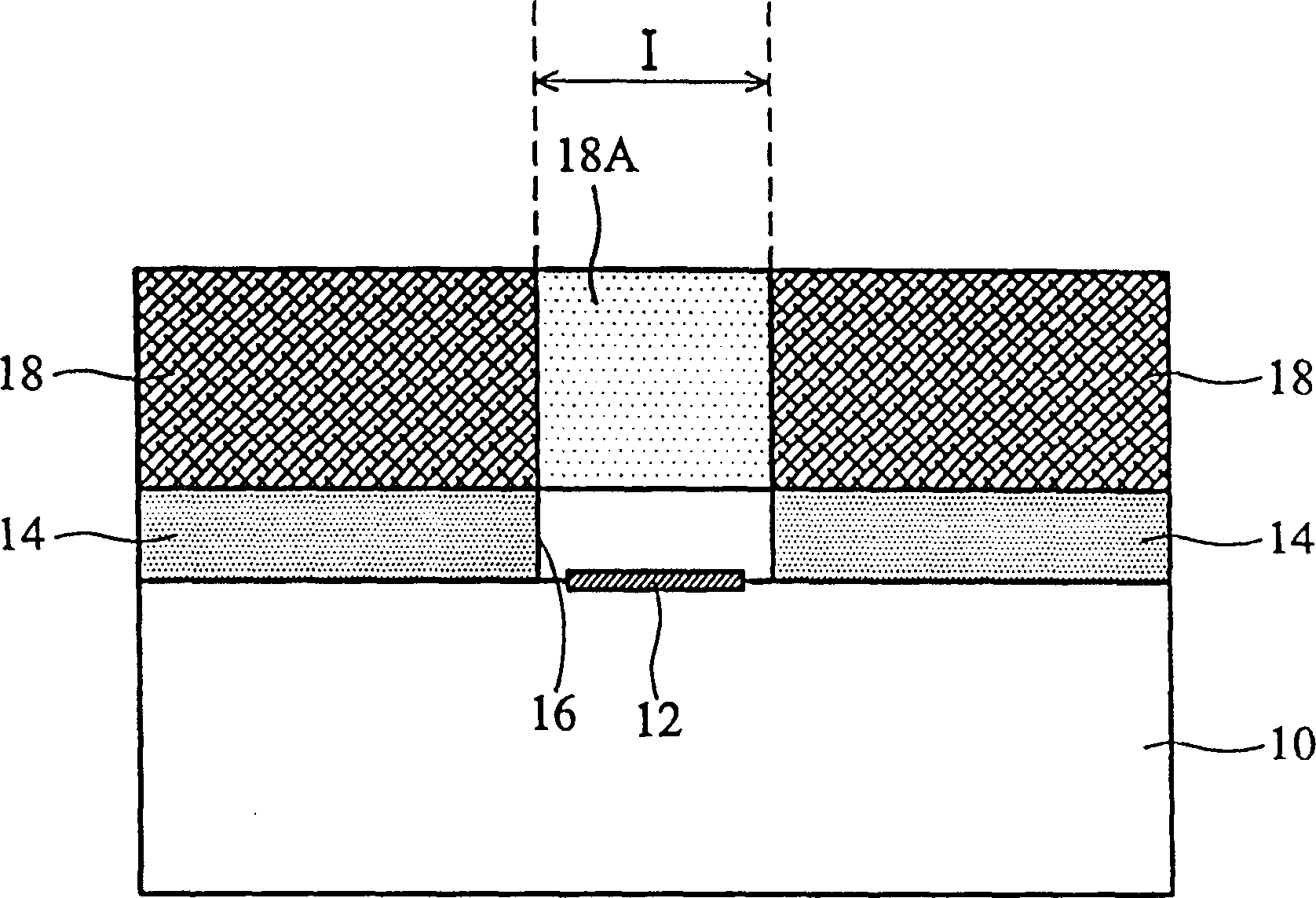
[0012] Figure 1A to Figure 1G It is a schematic cross-sectional view of an orifice sheet for making an inkjet print head according to the first embodiment of the present invention. first, Figure 1A As shown, a semiconductor silicon substrate 10 is provided, and its surface includes at least one actuating component 12 (for example: a thin film heater), and then a first thin film 14 is covered on the surface of the silicon substrate 10 by pressing film or other deposition methods. , its material can be selected from photosensitive polymer materials, such as: epoxy resin (epoxy), phenolic resin (novolak), acrylic resin (arcylate), polyimide (polyimide), polyamide (polyamide) or Photosensitive polymer material. Next, if Figure 1B As shown, the first film 14 in the first predetermined area I is exposed and developed to form a first opening 16 in the first film 14, and its position is corresponding to the top of the actuator assembly 12. For use as an ink channel (ink channel)...
no. 2 example
[0017] Figure 2A to Figure 2G It is a schematic cross-sectional view of an orifice sheet for making an inkjet print head according to the second embodiment of the present invention. First, if Figure 2A As shown, a semiconductor silicon substrate 30 is provided, and its surface includes at least one actuating component 32 (for example: a thin film heater), and then a first thin film 34 is covered on the surface of the silicon substrate 30 by pressing film or other deposition methods. , the material can be selected from photosensitive polymer materials, such as epoxy resin, phenol resin, acrylic resin, polyimide, polyamide or photosensitive polymer materials. Next, the exposure and development processes are carried out on the first thin film 34 in the first predetermined area I, so as to form a first opening 36 in the first thin film 34, and its position is corresponding to the top of the actuating component 32, which can be used Used as an ink channel.
[0018] follow, suc...
no. 3 example
[0022] In order to further simplify the manufacturing process of the orifice sheet in the second embodiment, the third embodiment of the present invention proposes another exposure and development step, which can be applied when the materials of the first film and the second film are different.
[0023] Figure 3A to Figure 3H It is a schematic cross-sectional view of an orifice sheet for making an inkjet print head according to the third embodiment of the present invention. First, if Figure 3A As shown, a semiconductor silicon substrate 40 is provided, and its surface includes at least one actuating component 42 (for example: a thin film heater), and then a first thin film 44 is covered on the surface of the silicon substrate 40 by pressing film or other deposition methods. , and its material can be selected from a polymer material with positive photoresist properties. Next, if Figure 3B As shown, the first exposure process is performed on the first thin film 44 in the f...
PUM
 Abstract
Description
Claims
Application Information