Method for selecting mask manufacturer for producing optical mask

A technology for manufacturers and photomasks, applied in the fields of original components for photomechanical processing, semiconductor/solid-state device manufacturing, optics, etc., can solve the problems of high mask prices and achieve the effect of easy selection of methods

Inactive Publication Date: 2004-01-21
MITSUBISHI ELECTRIC CORP
View PDF1 Cites 0 Cited by
  • Summary
  • Abstract
  • Description
  • Claims
  • Application Information

AI Technical Summary

Problems solved by technology

In this case, although the mask manufacturer can get a marginal profit corresponding to the difference in chip area, the result is that the mask price remains high

Method used


Image

  • Method for selecting mask manufacturer for producing optical mask
  • Method for selecting mask manufacturer for producing optical mask
  • Method for selecting mask manufacturer for producing optical mask

Examples


no. 1 Embodiment

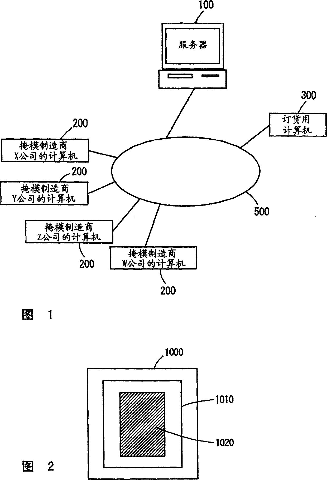
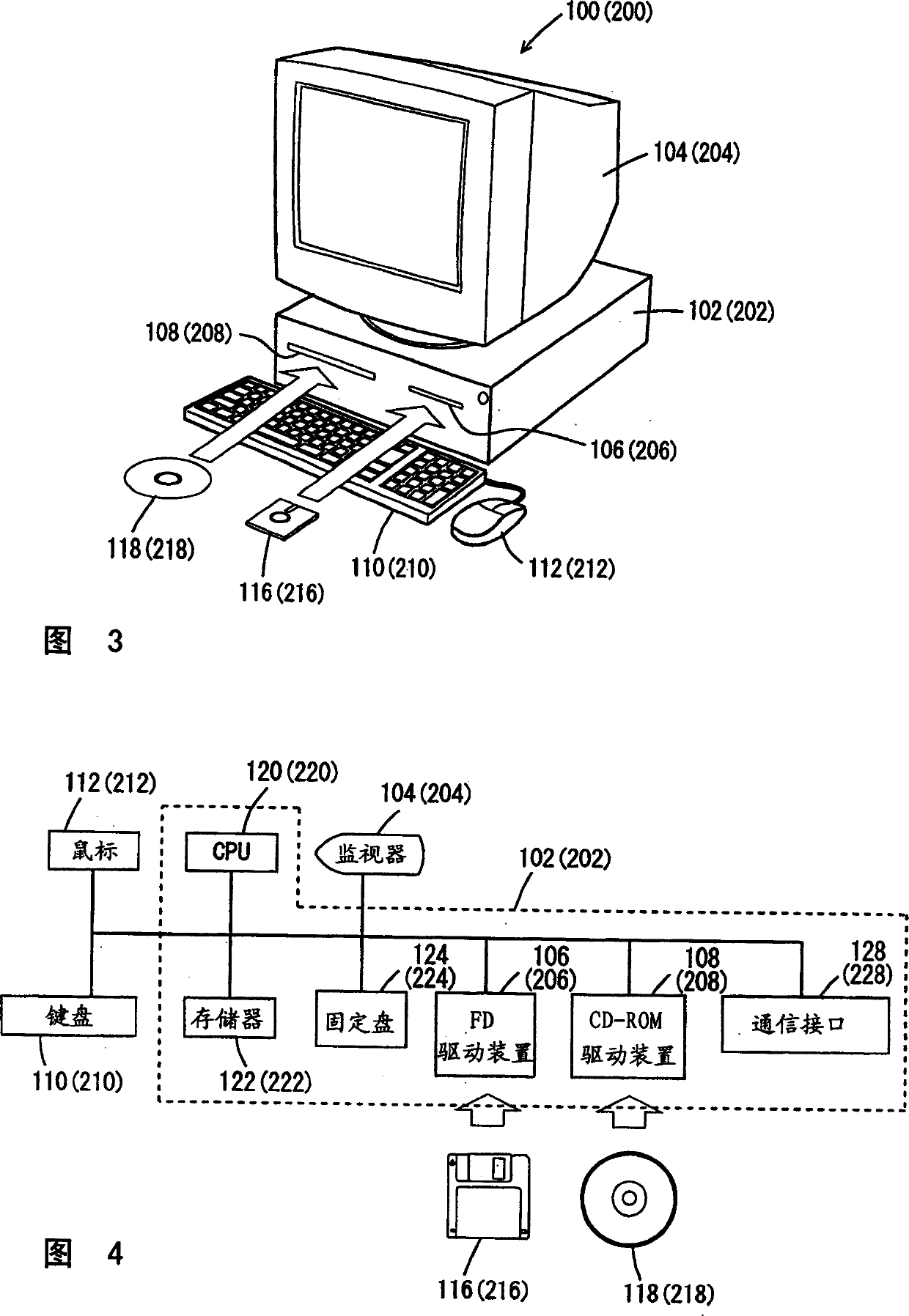
[0029] With reference to Fig. 1, the mask manufacturer selection system of the present embodiment comprises: the computer 200 of a plurality of mask manufacturers who manufacture photomask; The ordering computer 300 of the manufacturer's computer 200; and the wafer manufacturer's server 100 connected to these computers via the network 500.

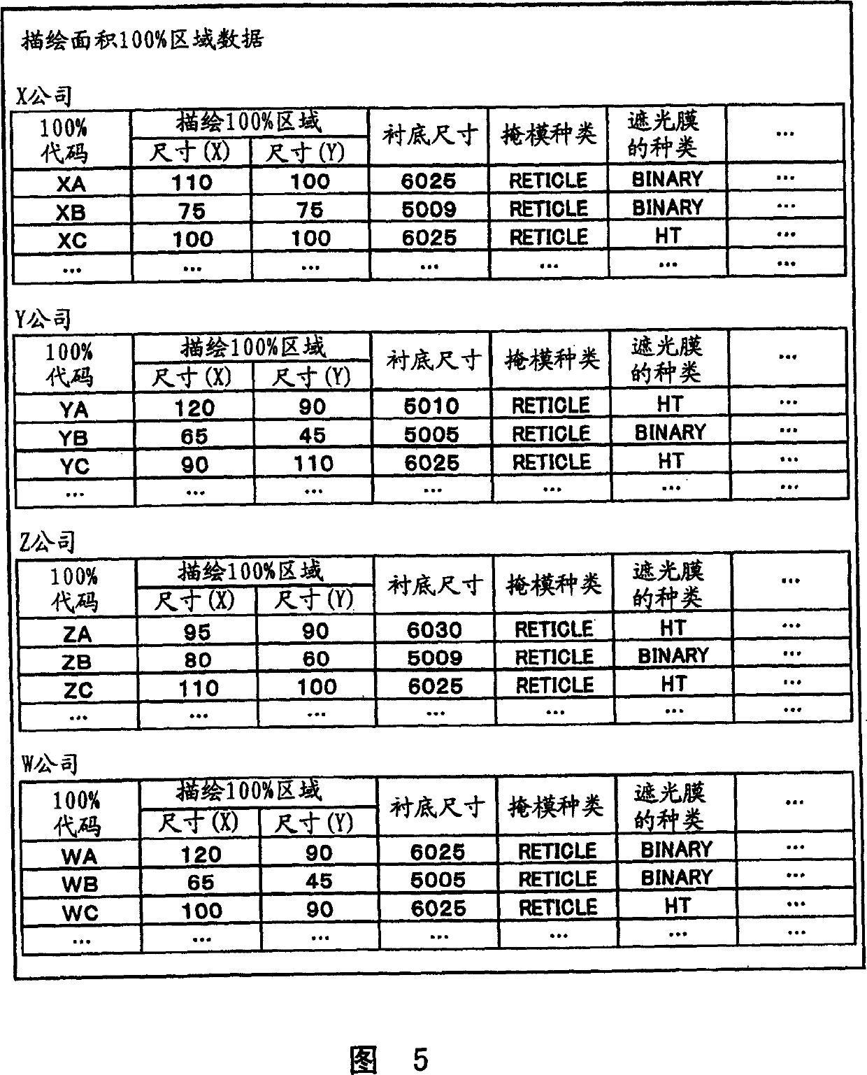
[0030] The server 100 stores order detail data including a drawing area of ​​a photomask. The computer 200 of the mask maker establishes and stores the maximum drawing area in the substrate on which the photomask is drawn as area data of 100% of the drawing area. The mask maker's computer 200 creates and stores unit price data of the photomask corresponding to the ratio of the drawing area of ​​the photomask to the maximum drawing area. These delineation area 100% area data and photomask unit price data are established for each mask maker.

[0031] Referring to FIG. 2 , the drawing area 100% area will be described. In the photomask 1000...

no. 2 Embodiment

[0082] Next, a mask maker selection system according to a second embodiment of the present invention will be described. Note that the hardware configurations of the wafer maker's server 100 and the mask maker's computer 200 other than the database and flowchart shown below are the same as those of the first embodiment described above. Therefore, detailed descriptions of them will not be repeated here.

[0083] Referring to FIG. 12 , the specification and use database will be described for each photomask process stored in the fixed disk 220 of the mask manufacturer's computer 200 . As shown in FIG. 12, for each mask name and process name, the database stores the chip size of the device, the order of photomasks used in the crystal wafer manufacturing process, the kind and arrangement of transfer marks, and photomask manufacturing conditions. , the purpose for which the device was manufactured, the period of manufacture and the destination of shipment of the device.

[0084] Re...


PUM


Abstract

A process for selecting a mask producer for semiconductor wafer photomask production from at least two masks comprises storing a maximum surface pattern for each, storing the relative cost based on the area ratio for the patterns, storing the specification data, finding the pattern forming ratio and selecting a mask on the basis of the price. An Independent claim is also included for an additional process using many patterns.

Description

technical field [0001] The present invention relates to a method for selecting an order-receiver of a photomask used as a master plate of a wafer for a semiconductor device in an ordering system for semiconductor devices, and particularly relates to a selection method capable of reducing the unit price of a photomask. Background technique [0002] Hitherto, IC (Integrated Circuit) chips provided with circuits whose wiring patterns are changed according to specifications required by customers have been produced by IC chip manufacturers (wafer manufacturers). Such an IC chip is manufactured by using a photomask in which a light-shielding pattern is formed with a metal thin film on a synthetic quartz substrate as a master plate in a photolithography process which is one of the manufacturing steps of an IC chip. The photomask is manufactured by a mask maker. The information related to the specifications is stored on a magnetic tape or the like, and is handed over from the wafer...

Claims


Application Information

Patent Timeline
IPC IPC(8): G03F1/68G06Q30/06G06Q50/00G06Q50/04H01L21/00H01L21/027
CPCG06Q30/0206G06Q10/087H01L21/00
Inventor 森正芳细野邦博有本一郎菊田裕子
Owner MITSUBISHI ELECTRIC CORP
Why Eureka
Try Eureka