

Ordered 2D and 3D nano structure metal material comprising hollow metal spheres and its prepn process
A nanostructure and metal material technology, applied in the field of ordered nanostructure metal materials, can solve problems such as difficulty in growing metals
- Summary
- Abstract
- Description
- Claims
- Application Information
AI Technical Summary
Problems solved by technology
Method used
Image

Examples
Embodiment Construction
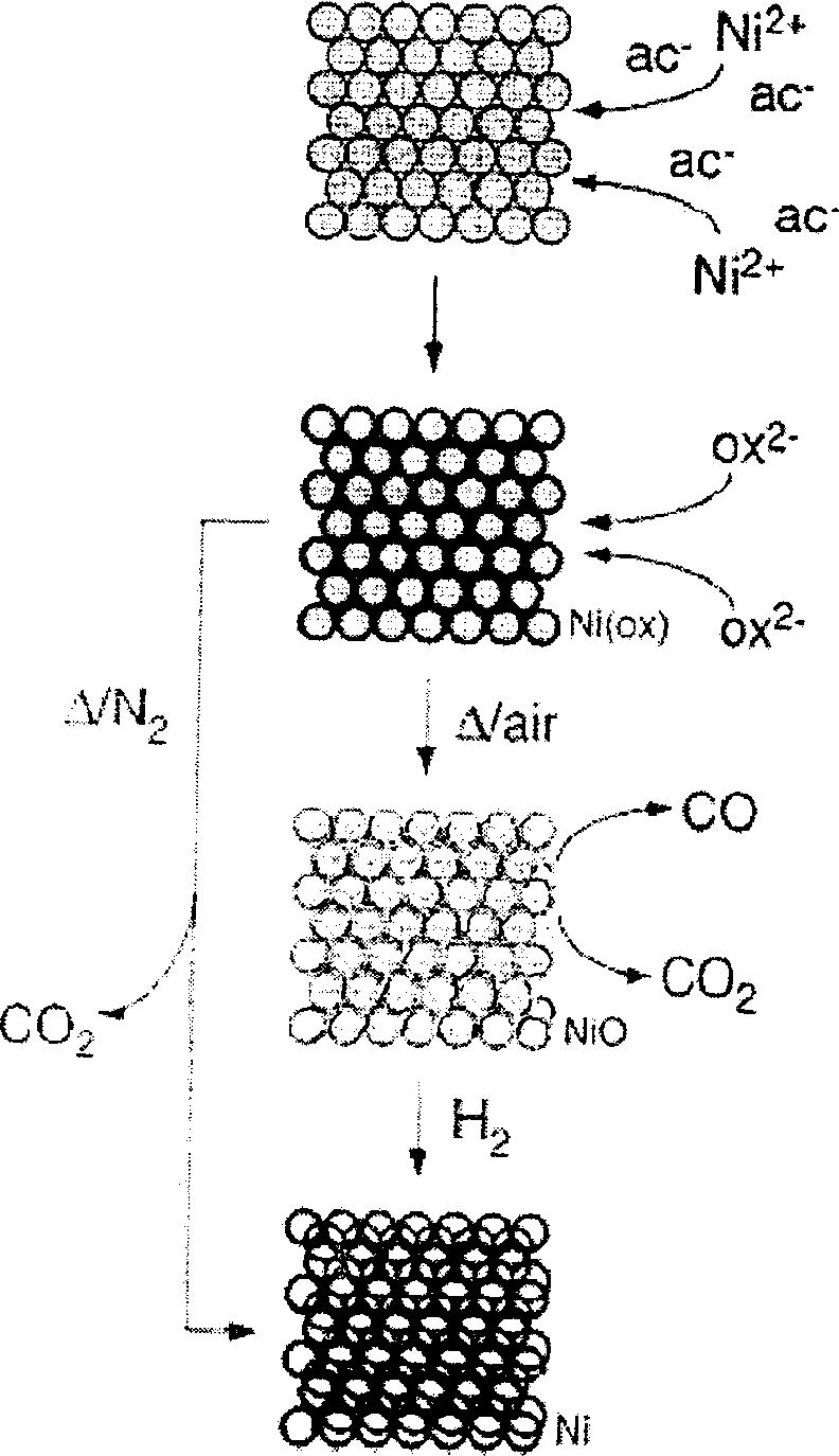
[0040] The schematic diagram of technological process of the present invention sees figure 2 .
[0041] The present invention first selects a wave plate as a substrate and lays it flat. Then two identical separators with a certain thickness are placed in parallel on the wave plate. Cover it with a wave plate of the same size. Finally, while maintaining the relative position of the two wave plates, fix them.
[0042] The separator in the present invention can be cylindrical or a dielectric rod with a rectangular cross section. The material of the spacer is selected from a dielectric material that can withstand a certain amount of extrusion without deformation.
[0043] The present invention can also use monodisperse silica spheres as spacers. The distance between two flat substrates is equal to the diameter of the silica sphere.
[0044] In the present invention, one end of the prepared microchannel is immersed in the configured colloidal microemulsion liquid. After the...
PUM
 Abstract
Description
Claims
Application Information