
Multiple quantum well structure and LED of the structure

A technology of light-emitting diodes and quantum wells, applied in phonon exciters, lasers, laser parts, etc., can solve the problems of small diffusion length, weakened radiation recombination, and reduced number of electrons and holes, so as to increase efficiency and enhance luminescence. the effect of strength

Inactive Publication Date: 2004-04-07
上海蓝宝光电材料有限公司
View PDF4 Cites 13 Cited by
  • Summary
  • Abstract
  • Description
  • Claims
  • Application Information

AI Technical Summary

Problems solved by technology

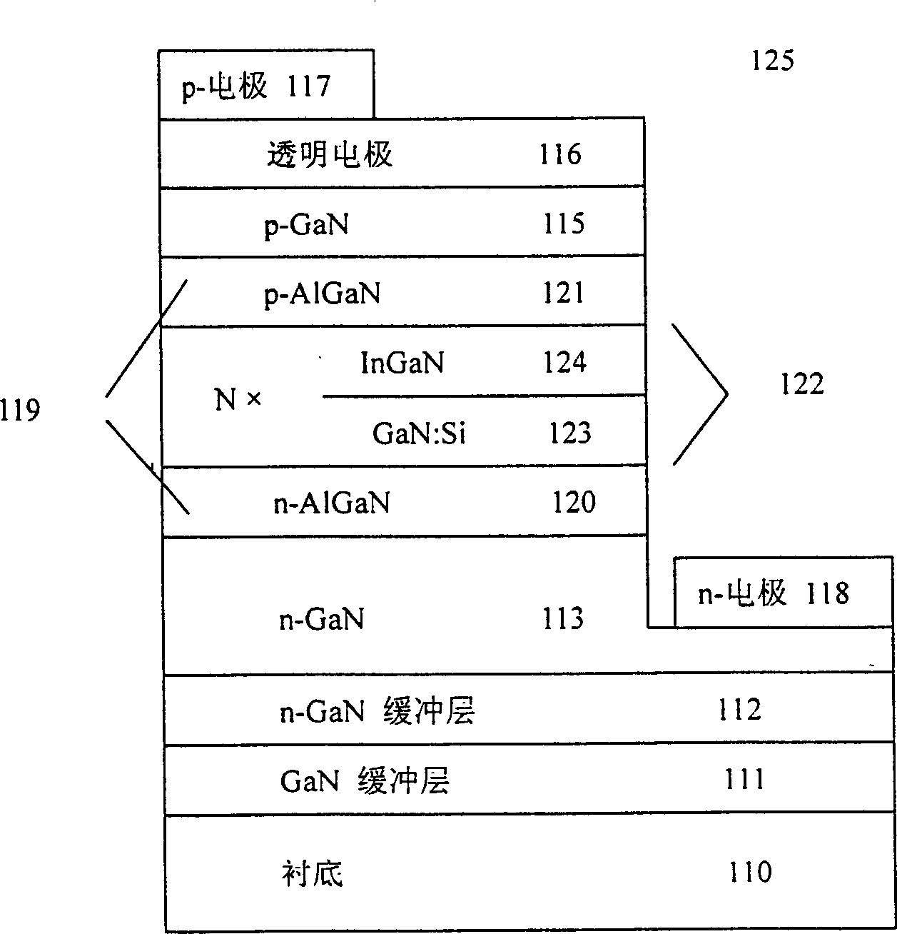
But this structure also has obvious disadvantages: first, the barrier doped with Si introduces n-type impurities in the quantum well, making the p-n junction deviate from the InGaN / GaN multi-quantum well region, so that when the light-emitting diode works in forward bias, The minority carriers in the quantum well region are holes, and the holes recombine with electrons to emit light during the diffusion process. However, due to the low mobility of the holes and the small diffusion length, the number of electrons and holes that undergo radiative recombination is correspondingly reduced. On the contrary, the minority carriers in the p-type doped GaN layer 115 are electrons, and their diffusion length is very long, which makes the recombination region mostly located in the p-type doped GaN layer 115, and occurs in the multiple quantum wells The radiative recombination is weakened; secondly, in this structure, when electrons and holes recombine, DA mainly emits light. With the increase of carrier injection, the DA center tends to be saturated, and the excess carriers will pass through the non-radiative The recombination process recombination greatly limits the further improvement of the luminous intensity of light-emitting diodes with InGaN / GaN multiple quantum wells as the active region

Method used


Image

  • Multiple quantum well structure and LED of the structure
  • Multiple quantum well structure and LED of the structure
  • Multiple quantum well structure and LED of the structure

Examples


Embodiment Construction

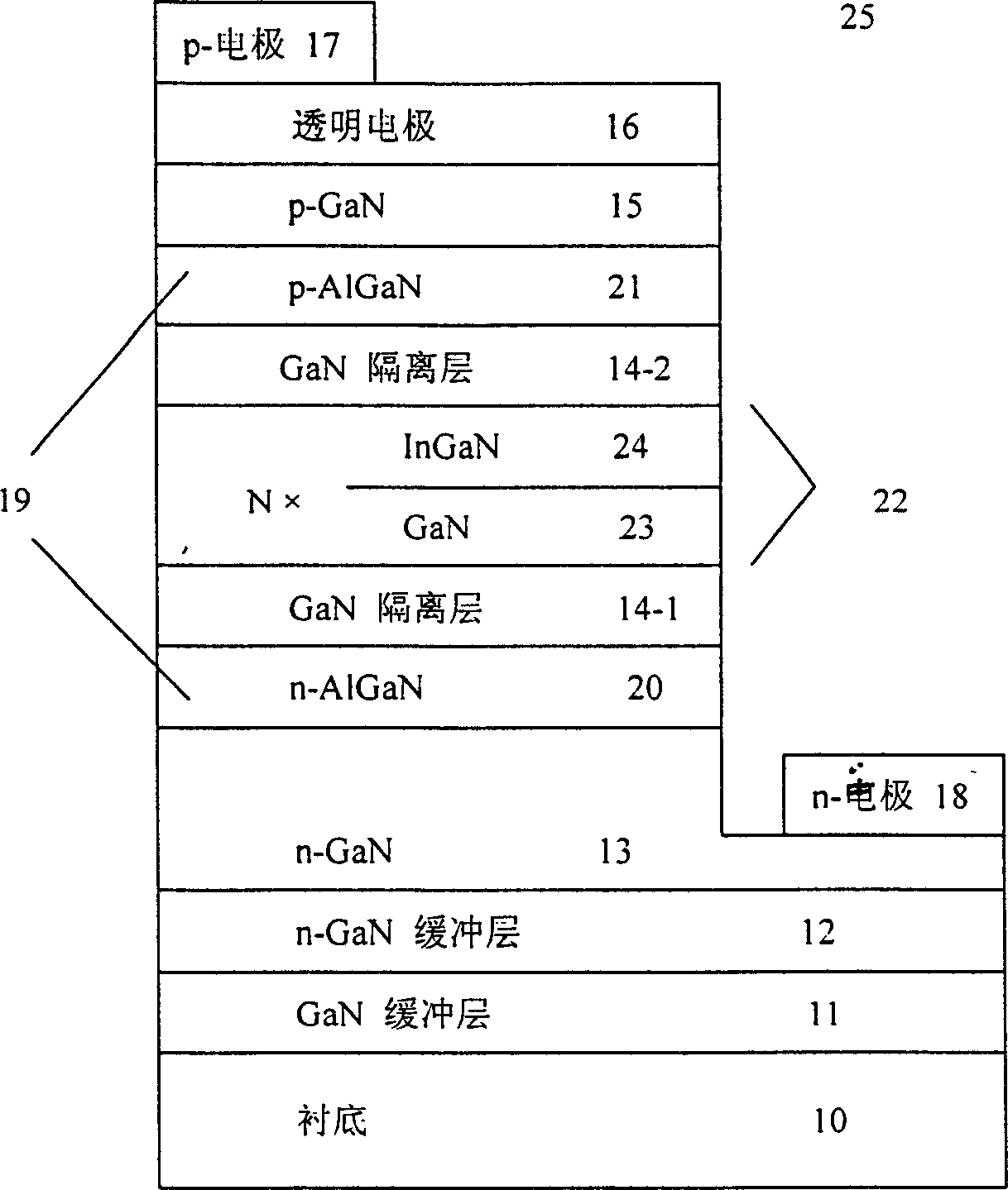
[0018] The GaN-based multi-quantum well blue light emitting diode 25 of the specific embodiment of the present invention, such as figure 2 shown. Wherein the multi-quantum well structure comprises: an AlGaN layer 19 comprising a p-type doped AlGaN layer 21, and an n-type doped AlGaN layer 20; between the p-type doped AlGaN layer 21 and the n-type doped AlGaN layer N quantum wells 22 between them, the quantum well structure in these N quantum wells comprises potential barrier layer 23 and potential well layer 24, and the bandgap of potential well layer 24 is smaller than potential barrier layer 23; In this p-type doped A GaN isolation layer 14-2 is also formed between the AlGaN layer 21 and the N quantum wells 22; a GaN isolation layer 14-1 is also formed between the n-type doped AlGaN layer 20 and the N quantum wells 22 .

[0019] In the above-mentioned GaN-based multiple quantum well structure, N in the N quantum wells 22 can be any integer from 1 to 100.

[0020] The bar...


PUM


Abstract

The present invention discloses one kind of multiple quantum well blue light GaN-base LED. The multiple quantum well structure of the LED includes: p-type doped AlGaN layer, n-type doped AlGaN layer, and N quantum wells comprising un-doped GaN layer and un-doped InGaN between the two A1GaN layers, as well as isolating un-doped GaN layer between the P-type doped A1GaN layer and the N quantum wells and isolating un-doped GaN layer between the n-type doped A1GaN layer and the N quantum wells. Regulating the thickness of the isolating un-doped GaN layers can regulate the position of p-n junction to the multiple quantum well region effectively and raise the light emitting strengt of the LED effectively.

Description

technical field [0001] The invention relates to a light-emitting diode, in particular to a light-emitting diode formed of a semiconductor material with sufficient wide bandgap to emit light in the green to violet part of the visible light spectrum and a multi-quantum well structure therein. Background technique [0002] Semiconductor light-emitting diode light sources have long life, low power consumption, and good reliability. They have been widely recognized in many fields of production and life, and have a wide range of uses. In the past ten years, short-wavelength light-emitting diodes represented by GaN-based blue light-emitting diodes have made great progress in basic research and commercial development, enabling humans to obtain high-repeatability, long-life panchromatic light sources including white light sources, the known GaN The base diode structure can refer to US Patents 4,918,497, 4,966,862, 5,027,168 and 5,338,944. [0003] The structure of GaN-based light-em...

Claims


Application Information

Patent Timeline
Patent Type & Authority Applications(China)
IPC IPC(8): H01L33/04H01S5/343
Inventor 陈弘贾海强周均铭韩英军于洪波黄绮
Owner 上海蓝宝光电材料有限公司
Learn More