Method for making polysilicon layer

A polysilicon layer and manufacturing method technology, which can be applied in the directions of polycrystalline material growth, chemical instruments and methods, crystal growth, etc., and can solve problems such as grain size limitation

Inactive Publication Date: 2004-06-02
AU OPTRONICS CORP
View PDF0 Cites 36 Cited by
  • Summary
  • Abstract
  • Description
  • Claims
  • Application Information

AI Technical Summary

Problems solved by technology

Since the openings 204 are arranged in an array, the grain growth in the x direction and the y direction is restricted by the adjacent openings 204. Therefore, although this method can effectively control the distribution of crystal nuclei, it is not effective for the crystal grains. size is still limited

Method used


Image

  • Method for making polysilicon layer
  • Method for making polysilicon layer
  • Method for making polysilicon layer

Examples


Embodiment Construction

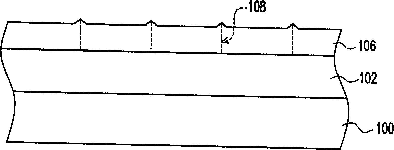
[0033] Figure 4 It is a schematic diagram of forming a polysilicon layer through a trench on a buffer layer according to a preferred embodiment of the present invention. Please refer to Figure 4 , providing a substrate 400, the substrate 400 is usually a glass substrate. Next, a buffer layer 402 is formed on the substrate 400 . The buffer layer 402 is, for example, a laminated structure including a silicon nitride layer and a silicon oxide layer (details will be described later). In order to improve the crystal size, uniformity and process margin in the formed polysilicon layer, in this embodiment, a plurality of parallel first trenches 404 are formed in the buffer layer 402, and these first trenches 404 are formed in the subsequent excimer In the laser thermal annealing process, it will play the role of providing crystallization nuclei. During excimer laser thermal annealing, the amorphous silicon layer (not shown) on the region outside the first trench 404 will be compl...


PUM


Abstract

The present invention discloses a method for making polycrystalline silicon layer which comprises, providing a substrate, forming a breaker having a plurality of ditches on the substrate, forming a non-crystalline silicon layer on the breaker, proceeding a laser annealing process to form a polycrystalline silicon. The invention can be applied into the production of low-temperature polycrystalline silicon thin film transistor LCDs.

Description

technical field [0001] The present invention relates to a method for making a polysilicon layer, and in particular to a polysilicon layer that takes an unmelted amorphous silicon layer in a trench (trench) as a nucleation site and undergoes lateral crystallization. Production Method. Background technique [0002] Low Temperature PolySilicon Liquid Crystal Display (LTPS LCD) is different from the general traditional amorphous silicon thin film transistor liquid crystal display (a-Si TFT-LCD), its electron mobility can reach 200cm 2 / V-sec or more, so the area occupied by the thin film transistor can be made smaller to meet the requirement of high aperture ratio, thereby improving the brightness of the display and reducing the overall power consumption problem. In addition, due to the increase in electron mobility, part of the driving circuit can be manufactured on the glass substrate together with the thin film transistor process, which greatly improves the reliability of th...

Claims


Application Information

Patent Timeline
Patent Type & Authority Applications(China)
IPC IPC(8): C30B28/02C30B29/06G02F1/13H01L21/283H01L21/324H01L21/44H01L21/477
Inventor 曹义昌
Owner AU OPTRONICS CORP
Why Eureka
Try Eureka