

Organic electroluminescence cell, planar light source and display device
A luminescent and organic technology, applied in the field of organic electroluminescent units, can solve problems such as high luminous efficiency
- Summary
- Abstract
- Description
- Claims
- Application Information
AI Technical Summary
Problems solved by technology
Method used
Image

Examples
Embodiment 1
[0202] The present invention is specifically described in the following Examples 1-1 to 1-6 and Comparative Examples 1-1 to 1-6, in which a light-diffusing layer (light-diffusing adhesive) or The lens structure acts as a reflection / refraction disrupting area.
Embodiment 1-1
[0204]
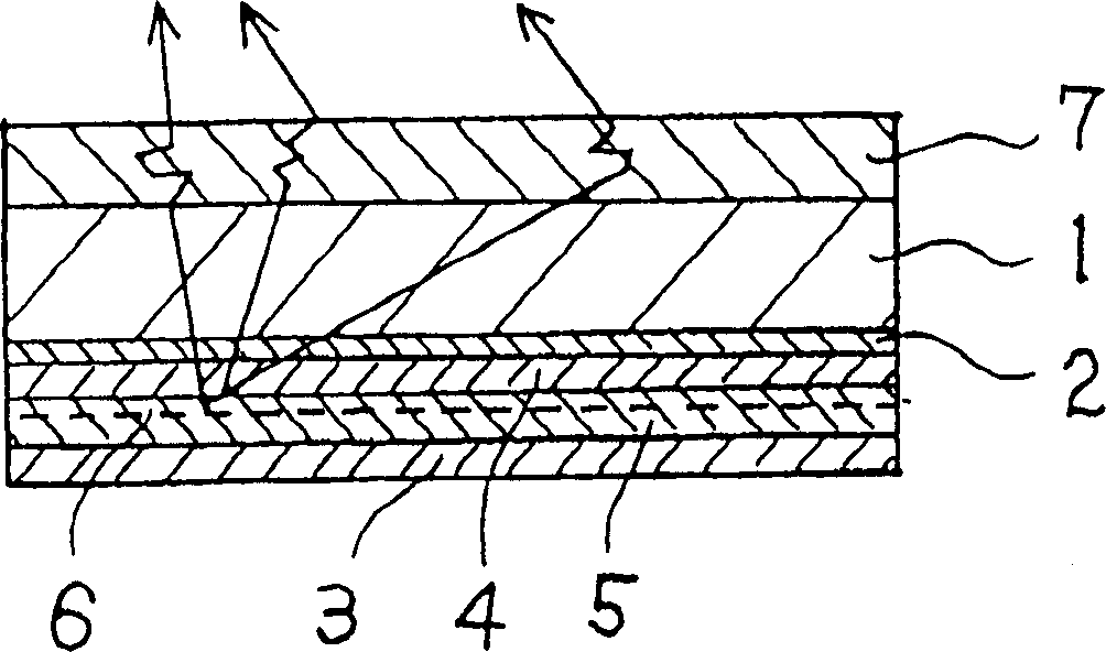
[0205] ITO ceramic targets (In 2 o 3 : SiO 2 =90% by weight: 10% by weight) to form a 100 nm-thick ITO film to form a transparent electrode (anode).
[0206] Then, under the condition of using a photoresist, the ITO was etched to form a pattern with a light emitting area of 15×15 mm. After ultrasonic cleaning, ozone cleaning is performed using a low-pressure UV lamp.
[0207] Organic layers were then successively formed on the ITO surface by vacuum vapor deposition. First, CuPc represented by formula (3) was deposited at a vapor deposition rate of 0.3nm / s to form a 15nm thick hole injection layer, and then CuPc represented by formula (4) was deposited at a vapor deposition rate of 0.3nm / s α-NPD to form a 40 nm thick hole transport layer. Finally, Alq represented by formula (5) was deposited at a vapor deposition rate of 0.3 nm / s to form a 140 nm-thick electron transport light-emitting layer.
[0208] Then, Mg and Ag were co-deposited at a vapor deposition ra...
Embodiment 1-2
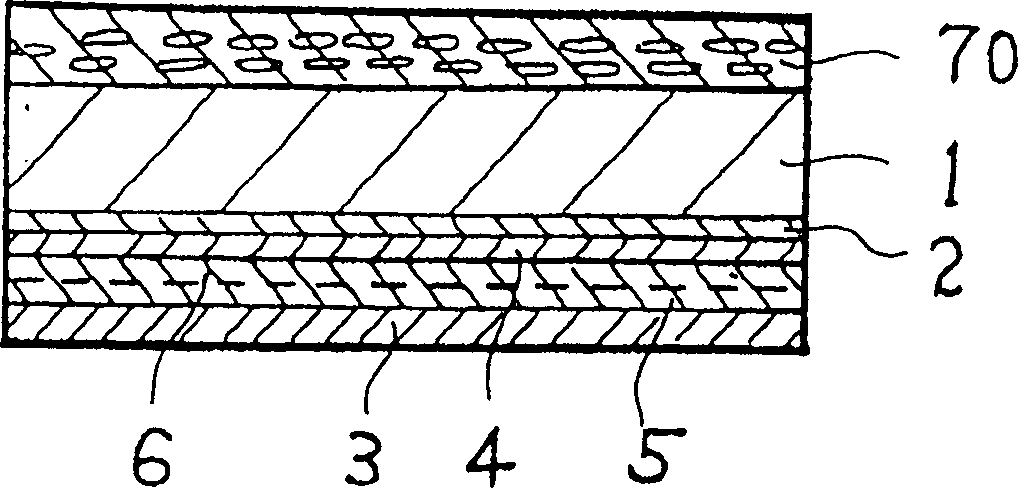
[0223] An organic EL unit as a basic structure and an organic EL unit including a light-diffusing layer added to the basic structure were produced in the same manner as in Example 1-1, but an Alq layer represented by formula (5) was formed with a thickness of 120 nm As an electron transport light-emitting layer.
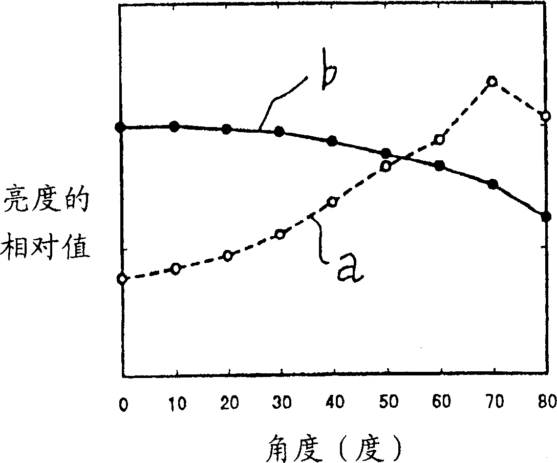
[0224] Before and after forming the light-diffusing layer, a voltage of 13.1 V was applied to the organic EL cell so that the current density was 10.5 mA / cm 2 An electric current flows in the cell to generate light in the same way. Under this condition, the organic EL unit was evaluated in the same manner as in Example 1-1. The evaluation results are shown in Table 1-2. Incidentally, the luminance distribution in the θ direction before forming the light-diffusing layer satisfies the relationship given by the expression (1) of the present invention, and the value of 120 nm as the thickness of the Alq layer also satisfies the relationship given by the expression (2) ...
PUM
| Property | Measurement | Unit |
|---|---|---|
| glass transition temperature | aaaaa | aaaaa |
| size | aaaaa | aaaaa |
| thickness | aaaaa | aaaaa |
Abstract
Description
Claims
Application Information