Method for producing N-type layer ohmic contact electrode of GaN LED

A technology of ohmic contact electrodes and light-emitting diodes, which is applied to circuits, electrical components, semiconductor devices, etc., and can solve problems such as not being on the same plane, affecting yield, and difficulty in bonding and flip-chip technology

Inactive Publication Date: 2004-09-01
INST OF SEMICONDUCTORS - CHINESE ACAD OF SCI
View PDF0 Cites 17 Cited by
  • Summary
  • Abstract
  • Description
  • Claims
  • Application Information

AI Technical Summary

Problems solved by technology

However, since the sapphire substrate is insulating, it is generally necessary to etch away part of the P-type layer and the light-emitting active region by etching or etching when making a light-emitting diode, exposing the N-type contact layer, and then preparing the N-type el...

Method used


Image

  • Method for producing N-type layer ohmic contact electrode of GaN LED
  • Method for producing N-type layer ohmic contact electrode of GaN LED
  • Method for producing N-type layer ohmic contact electrode of GaN LED

Examples


Embodiment Construction

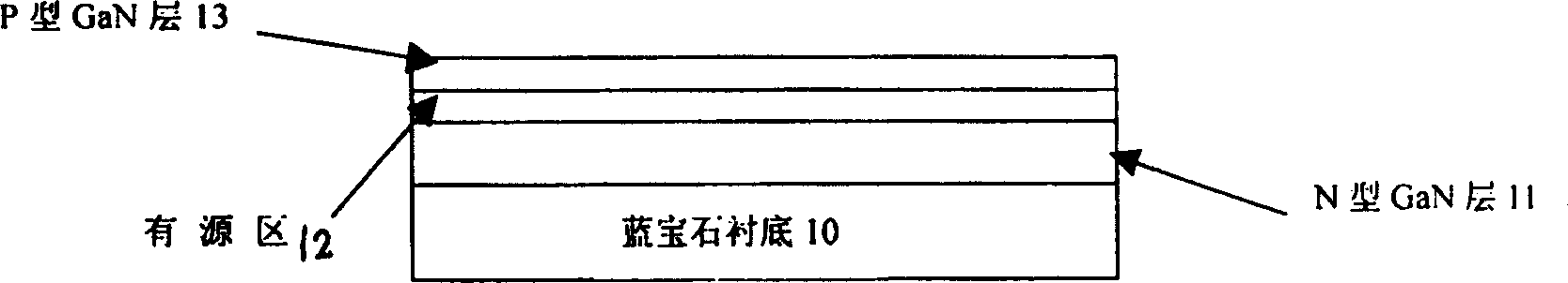
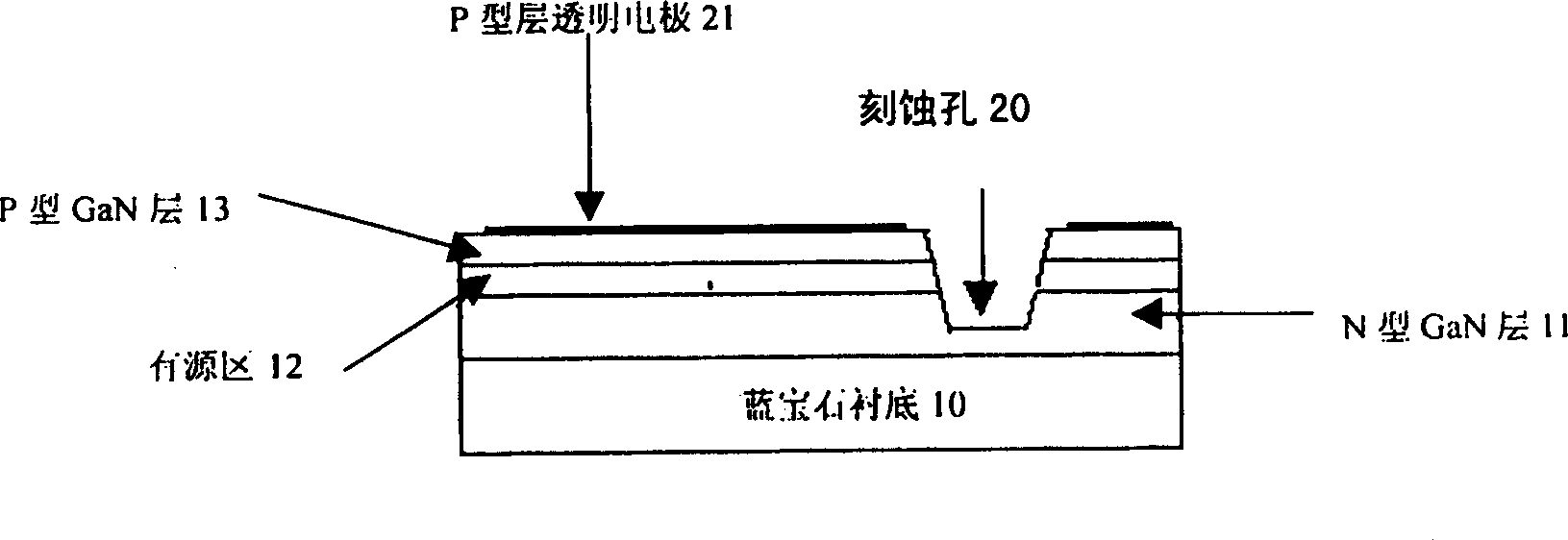
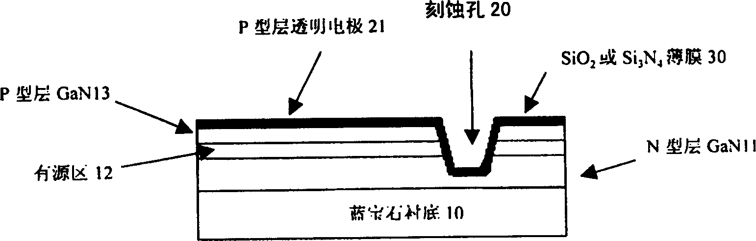
[0022] see figure 1 As shown, the fabrication method of the N-type layer ohmic contact electrode of the GaN-based light-emitting diode of the present invention generally includes forming an N-type GaN layer 11, an active layer 12 and a P-type GaN layer 11 on a sapphire substrate 10 by means of epitaxy. GaN layer 13.

[0023] First etch or corrode an etching hole 20 with a diameter of 30 microns at the N electrode position of the tube core design until the N-type layer 11 is exposed, and prepare the P-type layer transparent electrode 21 by photolithography and evaporation or sputtering, such as figure 2 shown;

[0024] Then use the CVD method to vapor-deposit a 0.10 micron silicon dioxide film 30 on the surface of gallium nitride, such as image 3 shown;

[0025] Then use photolithography and chemical etching to etch away the insulating film 30 on the surface of the N-type layer 11 and the area other than the N electrode. The diameter of the remaining insulating film 30 is ...


PUM

PropertyMeasurementUnit
Thicknessaaaaaaaaaa

Abstract

The invention is a manufacturing method for gallium nitride base brightening dioxide N type ohm contact electrode. It includes following steps: 1)etches out circle or rectangular or any shape hole whose diameter or side length is less than 50 um on the N electrode area of designed pipe core with dry etching method or humidity corroding method on the extension structure of gallium nitride base brightening dioxide on the sapphire substrate, etches to the N type contact layer; 2) produces a layer of P type transparent electrode on P type gallium nitride layer; 3) evaporates insulating film such as silicon dioxide or silicon nitride on the sample; 4) corrodes off the insulating film on N type layer etched or corroded with the photoetching method or corrosion method, and exposes N type layer, maintains the insulating film whose diameter or side length is about 100 um on the platform or side walls of the hole; 5) finally uses photoetching and evaporation or spattering method to produce N electrode, forms the gallium nitride base brightening dioxide N type ohm contact electrode.

Description

technical field [0001] The invention belongs to the technical field of semiconductors, in particular to a method for manufacturing an N-type layer ohmic contact electrode of a gallium nitride-based light-emitting diode on a sapphire substrate. Background technique [0002] III-V gallium nitride (GaN)-based compound semiconductors and their quantum well structure light-emitting diodes (LEDs) have the advantages of high reliability, high efficiency, fast response, long life, full solidification, and small size. , traffic light information indication, especially in the field of white light lighting has a huge application market. However, since the sapphire substrate is insulating, it is generally necessary to etch away part of the P-type layer and the light-emitting active region by etching or etching when making a light-emitting diode, exposing the N-type contact layer, and then preparing the N-type electrode , This manufacturing method reduces the effective light-emitting ar...

Claims


Application Information

Patent Timeline
IPC IPC(8): H01L21/28H01L33/00
Inventor 杨辉张书明
Owner INST OF SEMICONDUCTORS - CHINESE ACAD OF SCI
Why Eureka
Try Eureka