Integrated coil inductors for ic devices

A technology of integrated circuits and coil components, used in inductors, fixed inductors, printed inductors, etc.

Inactive Publication Date: 2004-09-01
GLOBALFOUNDRIES INC
View PDF0 Cites 1 Cited by
  • Summary
  • Abstract
  • Description
  • Claims
  • Application Information

AI Technical Summary

Problems solved by technology

These devices have some limitations due to the high capacitive coupling between the solenoid coils due to the very small overall thickness of the BEOL, about 8 to 10 microns, so the solenoid coils must be very close to each other in the vertical direction

Method used


Image

  • Integrated coil inductors for ic devices
  • Integrated coil inductors for ic devices
  • Integrated coil inductors for ic devices

Examples


Embodiment Construction

[0023] The present invention provides a multi-turn solenoidal inductor integrated in a semiconductor chip and its manufacturing method, which will now be described in more detail with reference to the accompanying drawings of this application. It should be noted that in the drawings, the same and / or corresponding components are marked with the same reference numerals.

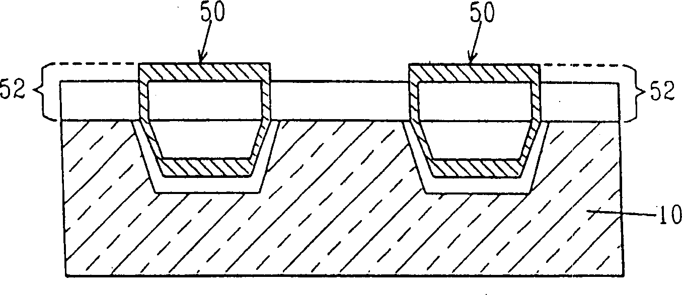
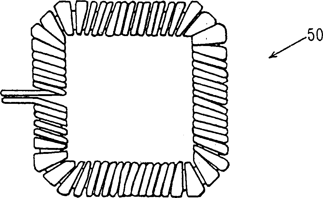
[0024] Reference is first made to the description of the semiconductor structure of the present invention Figure 1A (cross-sectional view) and 1B (top view). specifically, Figure 1A The structure in includes a substrate 10 having one or more solenoidal coils 50 formed in cavities formed in the substrate, partly in a BEOL wiring layer 52 . as an example, Figure 1A A top view of the solenoid coil 50 is shown in Figure 1B middle.

[0025] According to the present invention, each solenoid coil 50 includes a lower coil assembly 22 and an upper coil assembly 30 , which are electrically connected via a side coil...


PUM

PropertyMeasurementUnit
thicknessaaaaaaaaaa
thicknessaaaaaaaaaa

Abstract

A means for fabrication of solenoidal inductors integrated in a semiconductor chip is provided. The solenoidal coil is partially embedded in a deep well etched into the chip substrate. The non-embedded part of the coil is fabricated as part of the BEOL metallization layers. This allows for a large cross-sectional area of the solenoid turns, thus reducing the turn-to-turn capacitive coupling. Because the solenoidal coils of this invention have a large diameter cross-section, the coil can be made with a large inductance value and yet occupy a small area of the chip. The fabrication process includes etching of a deep cavity in the substrate after all the FEOL steps are completed; lining said cavity with a dielectric followed by fabrication of the part of the coil that will be embedded by deposition of a conductive material metal through a mask; deposition of dielectric and planarization of same by CMP. After planarization the fabrication of the remaining part of the solenoidal coil is fabricated as part of the metallization in the BEOL (i.e. as line / vias of the BEOL). To further increase the cross section of the solenoidal coil part of it may be built by electrodeposition through a mask on top of the BEOL layers.

Description

technical field [0001] The present invention relates to semiconductor devices, and more particularly, to multi-turn solenoidal inductors integrated in semiconductor chips, such as those used for radio frequency (RF) communications. The present invention also relates to a method of manufacturing novel multi-turn solenoidal inductors. Background technique [0002] Inductors integrated in semiconductor chips are generally fabricated in a BEOL (back-end-of-the-line) metallization plane (plus via holes to connect to or from the return arm) in a spiral shape. ))middle. Spiral inductors have relatively high impedance (about 1-5 ohms or more) for a given inductance value because of the thickness limitation of the BEOL metallization layer (about 2 to microns). Bimetallic layers with interconnecting via holes are sometimes used to reduce the spiral resistance. Because the inductance value is directly related to the length of the inductor threads, spiral inductors are limited to rel...

Claims


Application Information

Patent Timeline
Patent Type & Authority Applications(China)
IPC IPC(8): H01F17/00H01F17/04H01F17/06H01F27/00H01F27/06H01F41/04H01L21/02H01L27/08
CPCH01L27/08H01L28/10H01F17/0033H01F17/0006H01F41/041H01L27/04H01L29/00
Inventor R·E·阿科斯塔M·L·卡拉索S·A·科德斯R·A·格罗韦斯J·L·伦德J·罗斯纳
Owner GLOBALFOUNDRIES INC
Why Eureka
Try Eureka