Low-temp. polycrystalline silicon film transistor and its polycrystalline silicon layer making method

A technology of polysilicon layer and manufacturing method, which is applied in semiconductor/solid-state device manufacturing, electrical components, static indicators, etc., can solve the problem of polysilicon layer with many defects, and achieve the effect of good characteristics

Inactive Publication Date: 2004-10-13
AU OPTRONICS CORP
View PDF0 Cites 22 Cited by
  • Summary
  • Abstract
  • Description
  • Claims
  • Application Information

AI Technical Summary

Problems solved by technology

However, the disadvantage of the metal-induced crystallization process is that there are too many defects in the grown polysilicon layer, and a high-temperature post-process, such as a rapid thermal process or laser annealing process, is required. laser annealing process
[0006] However, taking the known active-matrix liquid crystal display as an example, the low-temperature polysilicon thin-film transistors in its peripheral circuits must have high electron mobility and on-state current; the display area (pixel area) must have The requirement of low leakage current; and the current polysilicon formed by the excimer laser annealing process cannot meet these two requirements at the same time

Method used


Image

  • Low-temp. polycrystalline silicon film transistor and its polycrystalline silicon layer making method
  • Low-temp. polycrystalline silicon film transistor and its polycrystalline silicon layer making method
  • Low-temp. polycrystalline silicon film transistor and its polycrystalline silicon layer making method

Examples


Embodiment Construction

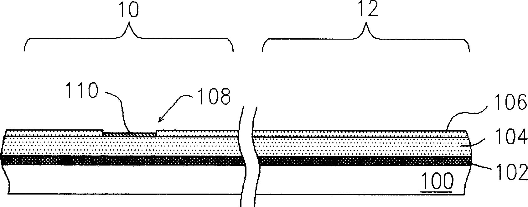
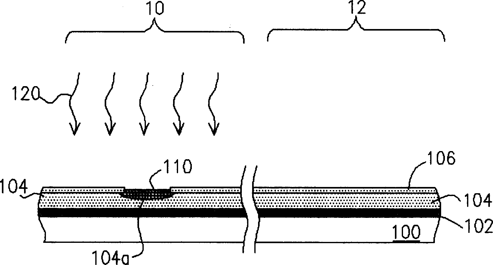
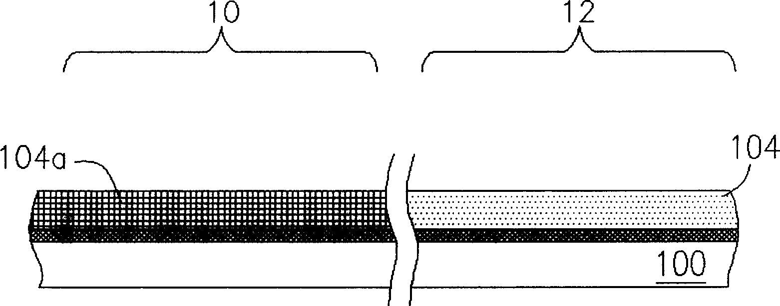
[0035] The present invention can be applied to low temperature polysilicon (low temperature poly-Si, LTPS for short) thin film transistor (thin film transistor, TFT for short), please refer to Figure 1A to Figure 1D , which is a sectional view of the manufacturing process of the polysilicon layer of the low temperature polysilicon thin film transistor according to a preferred embodiment of the present invention.

[0036] Please refer to Figure 1A First, selectively form a buffer layer (buffer layer) 102 on a panel 100, wherein the buffer layer 102 is, for example, a stacked layer composed of a silicon nitride layer and a silicon oxide layer, and its function is to improve the performance of the panel 100 and subsequent formation. Adhesion of the polysilicon layer and when there are metal ions such as sodium in the panel 100, it is used to prevent the metal ions in the panel 100 from contaminating the polysilicon layer. Then, an amorphous silicon (a-Si) layer 104 is formed on...


PUM

PropertyMeasurementUnit
electron mobilityaaaaaaaaaa

Abstract

The invention provides a low-temperature polycrystalline silicon film transistor and its polycrystalline silicon layer making method. First, form a noncrystalline silicon layer on a panel which including a display region and a peripheral circuit region. Then, form a metal layer on a part of the noncrystalline silicon layer in peripheral circuit region, then crystallize to make the other part form a polycrystalline silicon layer. Successively, make a quasi-molecular laser annealing processing to largen the crystal particles on the polycrystalline silicon layer and make the noncrystalline silicon layer in the display region into a polycrystalline silicon layer. Because the crystal particles of polycrystalline silicon in the peripheral circuit region are larger than those in the other parts, it can meet the demand of high-electron mobility. And because the crystal particles of polycrystalline silicon are smaller, it can meet the demand of low-leakage current.

Description

technical field [0001] The present invention relates to a method for manufacturing a low temperature polysilicon (LTPS) thin film transistor (thin film transistor, referred to as TFT), and in particular to a method for manufacturing a polysilicon layer in a low temperature polysilicon thin film transistor. Background technique [0002] With the development of high technology, video products, especially digital video or image devices have become common products in daily life. In these digital video or image devices, the display is an important component to display relevant information. Users can read information from the display, or further control the operation of the device. [0003] Thin-film transistors (TFT) can be applied to drive components of liquid crystal displays (LCDs for short), making this product the mainstream of straight flat-panel displays on desktops, and becoming a popular choice in markets such as personal computers, game consoles, and monitors. Future ...

Claims


Application Information

Patent Timeline
Patent Type & Authority Applications(China)
IPC IPC(8): G02F1/133H01L21/20H01L21/324H01L21/336
Inventor 彭佳添吴焕照
Owner AU OPTRONICS CORP
Why Eureka
Try Eureka