Photoelectric detector for 650nm optical fiber communication and its producing method

A photodetector and optical fiber communication technology, applied in the field of photodetectors, can solve the problems of reduced minority carrier diffusion length and low short-wave photoresponsivity

Inactive Publication Date: 2004-12-15
XIAMEN SAN U OPTRONICS
View PDF0 Cites 7 Cited by
  • Summary
  • Abstract
  • Description
  • Claims
  • Application Information

AI Technical Summary

Problems solved by technology

[0005] The existing photodetector for 650nm optical fiber communication is P + /I(N - )/N + Three-layer structure, its short-wave photoresponsivity is low, the reason is that the light surface P + The P-type

Method used


Image

  • Photoelectric detector for 650nm optical fiber communication and its producing method
  • Photoelectric detector for 650nm optical fiber communication and its producing method
  • Photoelectric detector for 650nm optical fiber communication and its producing method

Examples


Embodiment Construction

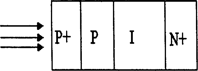
[0049] see figure 1 , the photodetector used for 650nm optical fiber communication is heavily doped P + Surface layer / P-type layer / Low-doped N - type epitaxial layer / heavily doped N + Substrate layer, namely P + / P / I(N - ) / N + Four layers of structure. After the P of the above structure + -P-I-N + The theoretical numerical simulation of the absolute spectral responsivity of silicon photodetectors with high and low emission junctions determines the vertical structure parameters of the device as:

[0050] P + The thickness of the zone is 0.1 μm and the concentration is 1×10 20 cm -3 , the thickness of the P region is 0.8 μm, and the concentration is 1×10 21 cm -3 , the thickness of I region is 200μm, N + The thickness of the zone is 0.5 μm and the concentration is 1×10 20 cm -3 , SiO 2 The film has a refractive index of 1.5 on SiO 2 The thickness of the film is 0.108 μm or 0.325 μm and the transmittance is 0.95%.

[0051] The parameters of the epitaxial wafer...


PUM

PropertyMeasurementUnit
Thicknessaaaaaaaaaa
Thicknessaaaaaaaaaa
Thicknessaaaaaaaaaa

Abstract

This invention relates to a photoelectric detector use in 650nm fiber communication compose of four layers of heavy doped p+ surface layer/P layer/light doped N- epitaxial layer/heavy doped N+ substrate in following steps: growing a material, oxidizing, photo etching the oxide film, diffusing the P type, evaporating the photo etched Al, forming an electrode with alloy, evaporating the O photo etched anti-reflection film and evaporating the back electrodes with good property of 1-v, small dark current and high light response. The heavy doped p+ surface layer is thin to reduce the 'dead layer' thickness and enables most part of incident light to pass through the p+ layer and inject into P layer and one layer to generate effective photo-generated carriers to improve the performance of the emitting region and increase the short wave quantum efficiency.

Description

technical field [0001] The invention relates to a photodetector, especially a photodetector used for 650nm optical fiber communication and a manufacturing method thereof. Background technique [0002] AlGaInP semiconductor laser with quantum well structure emits 650nm red light, which has been industrialized and mass-produced. As a red laser light source, it is widely used in DVD, VCD, CD and other audio-visual equipment, computer CD-ROM discs and optical reading devices for various laser barcodes. In addition, 650nm is a low-loss window for plastic optical fiber (M.Hayashi, M.Tsuji, K.Makita et al, GaAs Pin-photodiodes with an AlGaInP window layer for usein 650nm wavelength GI-POF data links.IEEE Photonic Technology Letters, 1996, 18, (6)) By further improving the performance of plastic optical fiber, such as reducing optical loss, increasing bandwidth and heat resistance, etc., it is expected to use 650nm plastic optical fiber communication to popularize fiber-to-the-home...

Claims


Application Information

Patent Timeline
IPC IPC(8): H01L27/14H01L31/08H01L31/105H01L31/18
CPCY02P70/50
Inventor 陈朝刘丽娜
Owner XIAMEN SAN U OPTRONICS
Why Eureka
Try Eureka